
Twisted Bilayer Graphene: A New Formula for Electron Lifetimes
Researchers derived an analytic formula for twisted bilayer graphene electron lifetimes, providing a key design tool for future quantum and electronic devices.
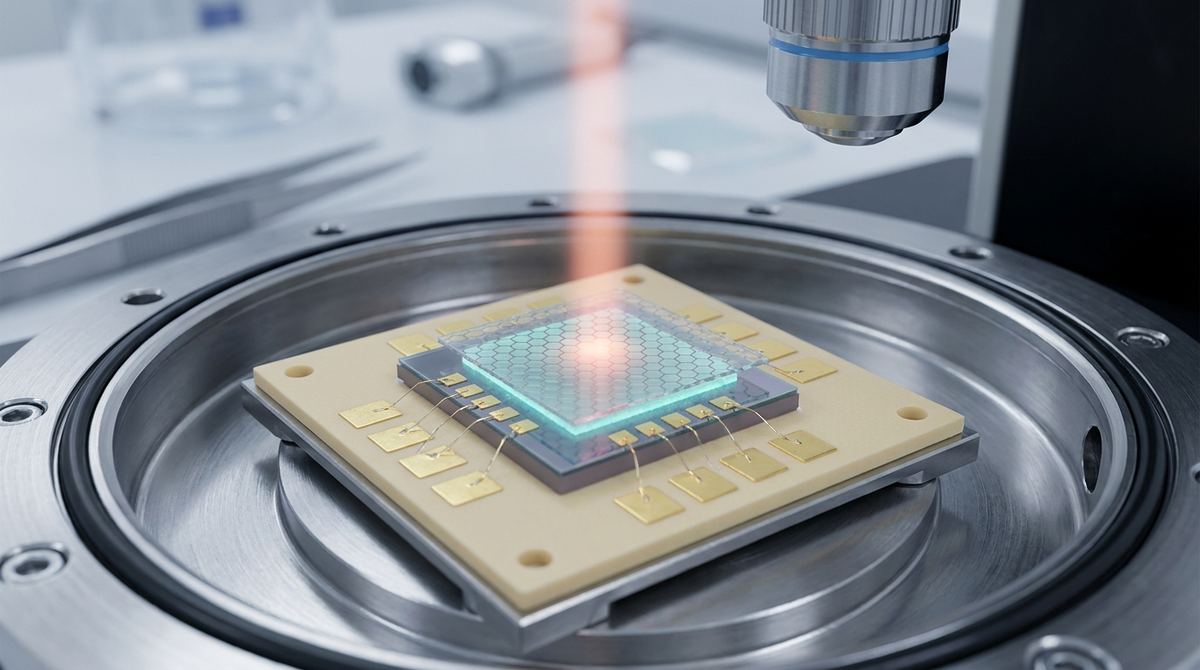
Detecting light in the short-wave infrared (SWIR) spectrum, specifically around the 1.5 µm (1550 nm) window, is critical for modern technology. This wavelength is the backbone of fiber optic communications, a preferred choice for eye-safe LiDAR systems, and essential for monitoring atmospheric gases. However, building detectors for this light is challenging. Standard silicon sensors are largely blind to it, and specialized materials like Indium Gallium Arsenide (InGaAs) are effective but prohibitively expensive for many applications.
A 2026 paper by Jinhua Wu and colleagues in Advanced Functional Materials presents an elegant and powerful solution that combines the unique properties of graphene with specialized nanoparticles. They developed a photodetector that achieves a record-breaking responsivity of 59.5 A/W for 1.5 µm light, using a surprisingly simple architecture. This performance leapfrogs many existing technologies and opens the door for low-cost, high-performance SWIR sensing.
This guide translates their research into a practical plan for building a prototype of this graphene-nanoparticle photodetector. We will walk through the device's operating principle, the necessary materials, a step-by-step fabrication process, and a plan for testing your prototype. This project is ambitious but achievable for a small lab, startup, or dedicated maker with access to basic fabrication tools.
The device's ingenuity lies in its hybrid structure and a clever two-step detection process. It isn't the graphene itself that directly detects the 1.5 µm photons. Instead, graphene acts as a powerful signal amplifier for a detection event happening in adjacent layers.
Here is the fundamental architecture:
1. Substrate: A standard silicon wafer (p-type, heavily doped) with a thin, insulating layer of silicon dioxide (SiO2) on top. This is a common platform in microelectronics.
2. Sensitizing Layer: A thin, uniform film of Erbium-doped upconversion nanoparticles (ENPs). In this case, the specific material is NaYF4:Er3+. These nanoparticles are the key to seeing the 1.5 µm light.
3. Active Channel: A single layer of high-quality graphene is placed over the nanoparticles and the substrate.
4. Contacts: Metal electrodes (Source and Drain) are patterned to make electrical contact with the graphene layer.
The detection mechanism works as follows:
1. Upconversion: When 1.5 µm infrared light hits the device, it passes through the transparent graphene and is absorbed by the ENPs. These nanoparticles are special; they absorb low-energy 1.5 µm photons and, through a process called upconversion, re-emit that energy as higher-energy photons at a shorter wavelength (around 980 nm).
2. Silicon Absorption: The underlying silicon substrate, which is insensitive to 1.5 µm light, is very good at absorbing this upconverted 980 nm light. This absorption generates electron-hole pairs within the silicon.
3. Photogating: The generated holes are driven by the device's electric field and become trapped at the interface between the silicon and the SiO2 layer. This accumulation of positive charge acts like a "photogate," strongly influencing the electrical properties of the graphene layer just above it.
4. Signal Amplification: The trapped positive charge induces a large number of negative charge carriers (electrons) in the graphene channel. This dramatically increases the graphene's conductivity. A single detection event (one trapped hole) can allow millions of electrons to flow through the graphene channel before it recombines. This is the source of the massive photoconductive gain (around 10^7) and the device's ultra-high responsivity.
Essentially, the ENPs act as translators, converting invisible SWIR light into a form the silicon can see, and the graphene acts as a massive amplifier, converting that small silicon signal into a large, easily measurable electrical current. This approach is a prime example of how nanomaterials can be combined to create devices with performance greater than the sum of their parts, a central theme in modern graphene electronics.
Building this device requires a combination of specialized materials and standard lab equipment.
Materials:
Substrate: A p-type, heavily doped silicon wafer with a 300 nm thermally grown SiO2 layer is a standard and suitable choice. The original paper used a specific resistivity, but a standard p++ wafer should be sufficient for a prototype.
Graphene: Monolayer CVD graphene grown on a copper foil. Quality is paramount here; look for suppliers that offer large, continuous films with low defect density.
Upconversion Nanoparticles: NaYF4:Er3+ nanoparticles (ENPs). This is the most specialized component. The paper reports synthesizing these via a hydrothermal method to achieve a high quantum yield of 2.1%. For a first prototype, synthesizing them may be out of scope. We recommend sourcing them from a specialty nanomaterial supplier. Ensure the emission spectrum under 1.5 µm excitation is verified by the supplier.
Solvents and Chemicals:
High-purity solvents for cleaning: Acetone, Isopropyl Alcohol (IPA), Deionized (DI) water.
Solvent for ENP dispersion: The paper used hexane. You may need to experiment to find the best solvent for the specific ENPs you source to achieve a stable, non-agglomerated suspension.
Chemicals for graphene transfer: PMMA (polymethyl methacrylate), copper etchant (e.g., ammonium persulfate or ferric chloride).
Metal for Contacts: Chromium (5 nm) as an adhesion layer and Gold (50 nm) for the main contact.
Equipment:
Cleaning: Ultrasonic bath, nitrogen gun.
Deposition: Spin coater, hot plate, e-beam or thermal evaporator for metal deposition.
Patterning: Access to a photolithography setup (mask aligner, developer) and reactive ion etcher (RIE) with oxygen is ideal. For a simpler prototype, a fine-tipped metal shadow mask can be used for electrode deposition.
Annealing: A tube furnace with controlled atmosphere capabilities (forming gas: 5% H2, 95% Ar or N2).
Testing:
Probe station for making electrical contact with the device.
Source Measure Unit (SMU), such as a Keithley 2400 or similar, to apply voltage and measure current precisely.
Laser Source: A tunable or fixed laser diode operating around 1.5 µm (1523 nm was used in the paper, but a standard 1550 nm telecom laser will work).
Optical Components: Lenses to focus the laser, an optical chopper, and a calibrated optical power meter.
Oscilloscope for measuring response time.
This process requires precision and cleanliness. Working in a cleanroom environment is highly recommended to minimize contamination, which can severely impact device performance.
1. Substrate Cleaning:
Begin with a thorough cleaning of the SiO2/Si wafer.
Sequentially sonicate the substrate in acetone, then IPA, for 10 minutes each.
Rinse thoroughly with DI water and dry with a gentle stream of nitrogen.
A final oxygen plasma ash or piranha clean (if available and you are trained in its use) can further remove organic residues.
2. Electrode Patterning:
The goal is to create two metal pads (source and drain) with a defined gap between them where the active channel will be.
Ideal Method (Photolithography): Spin-coat a photoresist, expose it with a photomask defining your electrode pattern, develop the resist, and then use an evaporator to deposit Cr/Au. A liftoff process in acetone will leave you with clean, well-defined electrodes.
Simpler Method (Shadow Mask): Securely place a pre-fabricated shadow mask with the desired electrode pattern onto your substrate. Place it in the evaporator and deposit the Cr/Au. This method is faster but yields less precise features. A channel length (gap between electrodes) of 10-50 µm is a good starting point.
3. ENP Layer Deposition:
Prepare a stable dispersion of the NaYF4:Er3+ nanoparticles in hexane. The paper used a concentration of 10 mg/mL. You may need to use an ultrasonic probe or bath to break up agglomerates.
Use a spin coater to deposit the ENP solution onto the substrate. The goal is a uniform, dense monolayer of nanoparticles covering the area between the electrodes.
Experiment with spin speed (e.g., 1000-4000 RPM) and time to achieve the desired film thickness and uniformity. After coating, gently bake on a hotplate at a low temperature (e.g., 90°C) for a few minutes to evaporate the solvent.
4. Graphene Transfer and Channel Definition:
This is a critical and delicate step in many graphene manufacturing techniques.
Spin-coat a support layer of PMMA onto the graphene/copper foil.
Float the foil on a copper etchant solution until all the copper is dissolved, leaving the graphene/PMMA film floating.
Carefully transfer the film to a DI water bath to rinse away etchant residue. Repeat this rinsing step 2-3 times.
Scoop the graphene/PMMA film out of the water using your device substrate.
Let it dry completely, then bake on a hotplate at around 150-180°C to improve adhesion.
Submerge the entire substrate in acetone to dissolve the PMMA support layer. This can take several hours or overnight. Finish with a rinse in fresh IPA.
To define the active channel, use photolithography and an oxygen plasma RIE to etch away the unwanted graphene, leaving only a strip of graphene connecting the source and drain electrodes.
5. Final Annealing:
This step removes residual contaminants from the transfer process and improves the electrical contact between the graphene, nanoparticles, and substrate.
Place the device in a tube furnace.
Anneal at 300°C for 2-3 hours in a forming gas (H2/Ar) atmosphere. Let it cool down slowly to room temperature before removing.
With the device fabricated, you can now characterize its performance.
1. Baseline Electrical Test:
Place the device on a probe station and connect the SMU to the source and drain electrodes.
In complete darkness, perform a voltage sweep (e.g., from -1 V to +1 V) and record the current. This gives you the I-V curve and the "dark resistance" of your graphene channel.
2. Photoresponse Measurement:
Set a constant bias voltage across the device (the paper found optimal performance at 1 V).
Measure the dark current (I_dark).
Focus your 1.5 µm laser onto the active area of the device. Measure the laser power hitting the device spot (P_incident) using your calibrated power meter.
With the laser on, measure the new current (I_light).
The photocurrent is calculated as: I_photo = I_light - I_dark.
Responsivity (R) is the key metric: R = I_photo / P_incident. The units are Amps per Watt (A/W). Don't be discouraged if your initial values are far from the paper's 59.5 A/W. Achieving such high performance requires significant optimization. Values in the range of 0.1 to 1 A/W would be a great success for a first prototype.
3. Response Time Measurement:
To measure how fast the detector responds, you need to modulate the laser beam. Use an optical chopper and connect the device output to an oscilloscope.
By observing the shape of the output current waveform, you can measure the rise time (10% to 90% of max signal) and fall time (90% to 10% of max signal). The paper reports millisecond-scale response, which is relatively slow but sufficient for applications like imaging and some types of sensing.
This guide simplifies a complex research process. It's important to acknowledge the assumptions and potential pitfalls.
Assumptions:
We assume you can source high-quality ENPs with good upconversion efficiency. The performance of the entire device hinges on this component.
We assume access to standard microfabrication equipment. If you are using simplified methods like shadow masks, expect lower performance and less device-to-device consistency.
The paper's record-high results are a product of meticulous optimization of every parameter: ENP synthesis, layer thicknesses, graphene quality, and interface cleanliness. Your first prototype is a proof-of-concept, not a record-breaker.
Risks and Mitigation:
Poor Graphene Quality: Wrinkles, tears, and polymer residue from the transfer process are the most common failure modes. They create scattering sites that reduce carrier mobility and overall performance. Mitigation: Practice the transfer process on dummy wafers. Use high-quality, large-area graphene. Perform the final anneal meticulously.
ENP Agglomeration: If the nanoparticles clump together instead of forming a uniform film, the upconversion process will be inefficient and non-uniform. Mitigation: Experiment with solvents and sonication methods to create a stable nanoparticle suspension before spin-coating.
High Dark Current: Contamination at the graphene/SiO2 interface can create charge traps that lead to a high baseline current, masking the photoresponse. Mitigation: Emphasize substrate cleaning and perform all fabrication steps in the cleanest environment possible.
Low Responsivity: This is the most likely initial result. It can be caused by any of the above issues, poor ENP quantum yield, or inefficient charge trapping at the interface. Mitigation: Treat this as an optimization problem. Systematically vary one parameter at a time (e.g., ENP concentration, annealing temperature) and re-test to find the optimal conditions. Exploring different material grades, such as turbostratic graphene flakes, could also be an interesting variable to test.
This practical guide is based on the findings published by Jinhua Wu et al. in their 2026 paper, "NaYF4:Er3+ Nanoparticles‐Graphene Photodetector for High‐Responsivity 1.5 µm Narrowband Imaging and Multi‐Wavelength Sensing." Their key contribution was the demonstration that combining highly efficient ENPs with a graphene photogating structure could overcome the traditional limitations of upconversion detectors, achieving unprecedented responsivity.
Once you have a working prototype, there are many exciting directions to explore. You could integrate the detector into a simple free-space optical communication system to transmit and receive a 1.5 µm signal. You could experiment with different types of upconversion nanoparticles to target other infrared wavelengths. Or, you could focus on optimizing the device architecture to improve response speed, which is currently a limiting factor. This project serves as an excellent platform for anyone interested in the practical application of advanced graphene sensors.
Serious about B2B integration? Test our premium Pulsed Electrical Resistive Carbon Heating turbostratic graphene in your lab. 100g sample packs available now.
Explore More
Researchers derived an analytic formula for twisted bilayer graphene electron lifetimes, providing a key design tool for future quantum and electronic devices.

New software for the modal analysis of electromagnetic resonators now includes 2D materials, accelerating the design of advanced graphene optical and...

New research provides a theoretical framework for calculating the lifetime and spectral function of topological heavy fermions, a key step for developing...