
Modeling Graphene Resonators: New Software Unlocks Advanced Optical Design
New software for the modal analysis of electromagnetic resonators now includes 2D materials, accelerating the design of advanced graphene optical and...
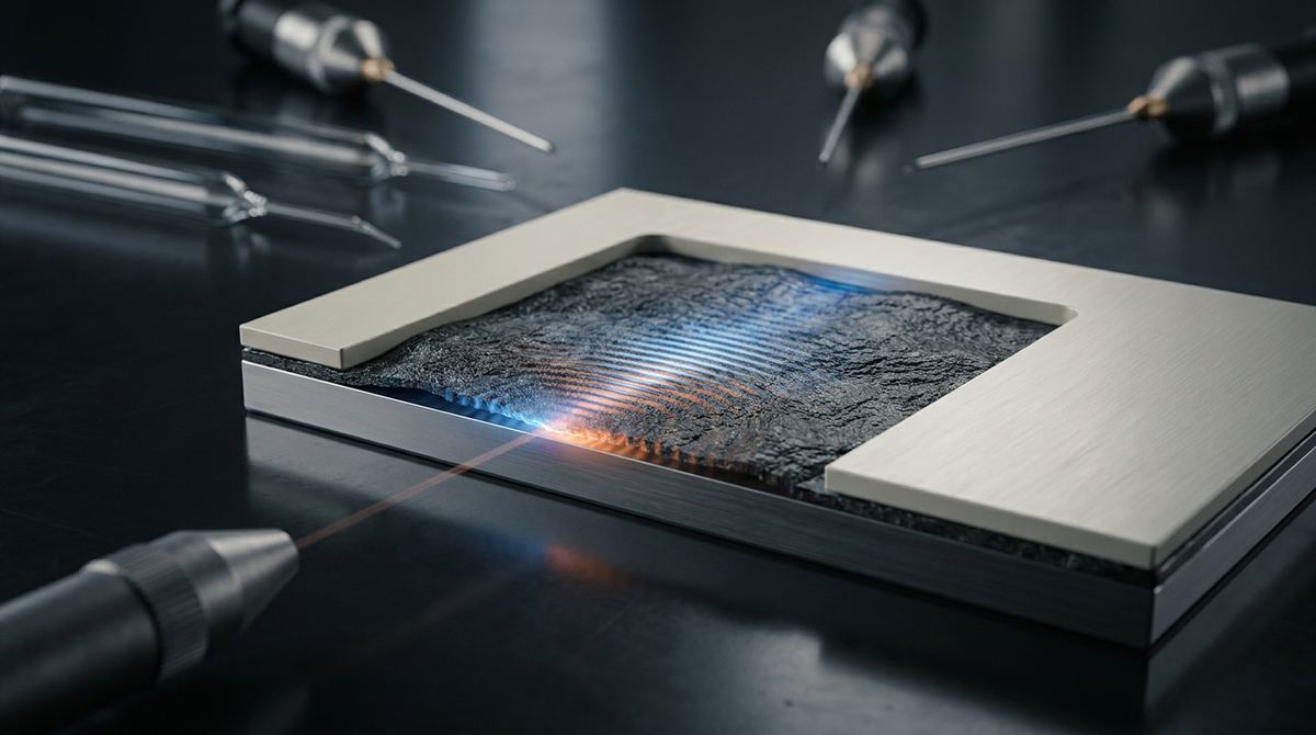
Imagine looking at a crowded ballroom through a camera that can only take one photo every ten minutes. You might see people in different spots, but you would never truly see the dance. You wouldn't see the graceful sway of an arm, the quick step of a foot, or the way a group of dancers moves in synchronization. In the world of materials science, atoms are those dancers. They are never truly still; they are constantly vibrating, shaking, and oscillating in complex patterns. These vibrations, known as lattice dynamics, dictate almost everything about how a material behaves, from how fast it conducts electricity to how well it dissipates heat. For decades, scientists have struggled to capture this dance because it happens at speeds far too fast for human eyes or even standard microscopes to see, and often at scales so small that the very act of looking changes the dance itself.
The fundamental challenge in modern condensed matter physics is the ability to observe atomic movement without disturbing the very process we are trying to study. When we attempt to measure the position of an atom, we must interact with it, usually by hitting it with a photon or an electron. However, if that interaction is too forceful, it knocks the atom out of its natural rhythm, effectively ruining the experiment. This is a manifestation of the uncertainty principle, where the act of measurement introduces energy into the system, making it difficult to distinguish between the natural thermal vibrations of the lattice and the vibrations caused by our measurement tools.
Furthermore, traditional measurement techniques often provide an average view of the material. If you use a method called X-ray diffraction, you are essentially looking at the "ensemble average" of billions of atoms. This tells you where atoms are likely to be on average, but it tells you nothing about what a single atom is doing at a specific moment in time. This lack of detail is a massive hurdle for engineers working on the cutting edge of nanotechnology. As electronic components shrink toward the atomic scale, the way heat moves through a material becomes localized. If heat is carried by specific vibrations called phonons, and those phonons are scattered by a single defect or a specific structural twist, an "average" measurement will miss the critical details that explain why a chip is overheating. We need to see the vibrations in real-space, meaning we know exactly where they are, and in real-time, meaning we know exactly when they happen.
The breakthrough concept explored in the work of Navdeep Rana involves breaking the historical barrier between seeing where an atom is and seeing when it moves. To do this, researchers use a technique that functions much like a high-speed strobe light used in photography. Instead of a continuous light that would wash out the movement, they use extremely short, incredibly fast pulses of light. These pulses are so brief—lasting only femtoseconds, which is a quadrillionth of a second—that they can "freeze" the motion of the atoms.
The strategy is to use one pulse to give the atoms a little "kick" to start a vibration, and then use a second, much weaker pulse to check on them a split second later. By varying the time delay between these two pulses, researchers can create a high-speed movie of the atomic dance. If the measurement can also be focused on a very tiny area, we achieve real-space resolution. This allows us to watch a single wave of vibration travel through a crystal lattice, much like watching a ripple move across the surface of a still pond. By mastering this, we move from seeing a blurry, static image of a material to seeing a dynamic, living map of energy in motion.
To understand how this works in a practical system, we must look at the unique properties of 2D materials like graphene. In a graphene lattice, carbon atoms are arranged in a perfect, flat hexagonal grid. Because it is only one atom thick, there is no "bulk" above or below the atoms, which makes it an ideal playground for observing how vibrations move through a two-dimensional plane.
The process begins with a "pump" pulse. This is a high-energy laser pulse that hits the graphene sample. This pulse doesn't just heat the material; it injects energy into the electronic system, which then transfers that energy into the atomic lattice. This creates a coherent phonon—a synchronized wave of atomic movement. Once this wave is traveling through the lattice, the "probe" pulse enters the scene. This pulse is much weaker to ensure it does not disrupt the system significantly.
The probe pulse measures how the material's optical properties change in response to the vibration. For example, as the atoms move closer together or further apart, the way the material reflects or absorbs light changes slightly. By measuring these tiny changes in light intensity or phase with extreme precision, the researchers can map out the movement. Because the laser can be focused to a spot only a few nanometers wide, the data captured is not an average of the whole sheet, but a precise map of the lattice dynamics at a specific coordinate. This combination of ultrafast timing and nanometer-scale focus is what allows for the simultaneous observation of real-space and real-time dynamics.
The research conducted by Navdeep Rana focuses on the intricate ways these vibrational wavepackets propagate through the crystal. The findings indicate that when a material is excited, the energy does not just dissipate randomly as heat. Instead, it travels in organized, coherent waves that can be tracked as they move away from the point of impact. The study demonstrates that by controlling the initial excitation, it is possible to observe how these vibrations interact with the specific geometry of the lattice.
A significant finding in this area of research is the observation of how phonons—the particles that represent these vibrations—interact with one another and with structural defects. The researchers were able to observe how a localized vibration spreads out across the real-space coordinates of the material over a period of picoseconds. This provides a direct visual confirmation of how energy is distributed in a low-dimensional system. This level of detail allows scientists to see how a single "ripple" of heat moves through the carbon atoms, providing a level of detail that was previously thought to be impossible due to the limitations of standard spectroscopic techniques. This research effectively bridges the gap between theoretical models of lattice vibrations and actual, observable physical reality.
The implications of being able to see atomic vibrations in real-time and real-space are profound, particularly for the future of computing and energy efficiency. One of the greatest challenges in modern microelectronics is the "thermal wall." As we pack more transistors into smaller areas, the heat generated by the movement of electrons becomes harder to remove. This heat is essentially a collection of chaotic atomic vibrations. If we can see exactly how these vibrations travel and where they get "stuck," we can engineer materials that guide heat away from sensitive components more effectively.
Furthermore, this research is vital for the development of new types of electronics, such as phononics. While electronics rely on the movement of electrons to process information, phononics aims to use the movement of atomic vibrations to carry information. This could lead to devices that are significantly faster and more energy-efficient than current silicon-based technology. By understanding the precise dynamics of how these vibrations move and interact, engineers can design "acoustic waveguides" for atoms, essentially creating highways for heat and information at the nanoscale. This level of control would revolutionize everything from high-performance supercomputers to the tiny sensors found in smartphones.
While the ability to probe lattice dynamics with such precision is a landmark achievement, it is important to note that this technology is currently in a highly controlled, fundamental research stage. The equipment required—ultrafast femtosecond laser systems and high-resolution detectors—is incredibly expensive and complex, making it difficult to use for routine industrial quality control at this time.
Additionally, there are significant challenges regarding sample preparation and stability. To see these dynamics clearly, the materials must be extremely pure and nearly perfect. Even a tiny amount of contamination from the air or a slight imperfection in the crystal structure can drown out the signals being measured. There is also the issue of the "observer effect" mentioned earlier; as we try to increase the resolution to see even smaller movements, the energy required to do so increases, which can fundamentally change the behavior of the material. Future research will need to focus on developing "non-invasive" or "ultra-weak" probing methods that can capture even more detail without perturbing the system, and finding ways to apply these techniques to less-than-perfect, real-world materials used in manufacturing.
The transition from laboratory observation to industrial application is a long road, but the potential applications are vast. In the realm of semiconductor manufacturing, the ability to map thermal dissipation at the atomic level could lead to the design of new heat-sinking materials that are integrated directly into the chip architecture. This would allow for much higher clock speeds in CPUs without the risk of thermal throttling or permanent hardware damage.
In the field of quantum computing, lattice dynamics are critical. Quantum bits, or qubits, are incredibly sensitive to their environment. Even a single stray phonon—a single atomic vibration—can cause "decoherence," where the quantum state of the qubit is lost, resulting in computational errors. By understanding the real-space and real-time movement of these vibrations, scientists can design better shielding and material structures to protect qubits, leading to more stable and powerful quantum computers. Additionally, in the field of advanced optics, these techniques can be used to develop new types of ultrafast light detectors and modulators, which are essential for the next generation of high-speed telecommunications and optical computing.
If there is one takeaway from this research, it is that the movement of atoms is not just random noise; it is a highly organized dance that dictates the limits of modern technology, and by learning to watch this dance in real-time and real-space, we unlock the ability to control the very foundations of matter.
What are lattice dynamics and why are they important?
Lattice dynamics refers to the study of how atoms within a crystal structure vibrate around their equilibrium positions. These vibrations are important because they are the primary carriers of heat and sound in solids. Understanding how these vibrations move is essential for controlling the temperature and electrical conductivity of materials used in electronics.
Why is it difficult to observe atoms moving in real-time?
Observing atoms in real-time is difficult because atomic vibrations occur at incredibly high frequencies, often on the scale of femtoseconds. Standard imaging techniques are far too slow to capture these movements. Furthermore, any attempt to observe them often requires hitting the atoms with energy, which can change the very movement the scientist is trying to measure.
What is the difference between real-space and real-time imaging?
Real-space imaging refers to knowing the exact physical location of an atom or a group of atoms at a specific point in the material. Real-time imaging refers to knowing exactly when a movement occurs. To truly understand material behavior, scientists need both: they need to know where the atoms are and exactly when they move.
How does this research relate to graphene and other 2D materials?
Graphene is a single layer of atoms, making it a perfect two-dimensional platform for studying vibrations. Because there are no layers above or below, researchers can observe how a vibration moves across the surface without it being muffled by a bulk material. This makes 2D materials ideal models for testing these advanced measurement techniques.
How could this research help make faster computers?
As computers get smaller, they generate intense heat that is difficult to manage. This heat is actually the movement of atoms (phonons). By using these new measurement techniques, engineers can see exactly how heat moves through a chip and design better ways to move that heat away, allowing the chip to run faster without overheating.
This research points toward a practical lesson: graphene-based materials are most powerful when their nanoscale properties are connected to a clear engineering problem. The result is not a finished commercial product by itself, but it gives researchers and manufacturers a better map for designing lighter, more sensitive, or more durable systems. Future work still needs testing under real operating conditions, but the direction is promising because it joins materials science with application-driven design.
Serious about B2B integration? Test our premium Pulsed Electrical Resistive Carbon Heating turbostratic graphene in your lab. 100g sample packs available now.
Explore More
New software for the modal analysis of electromagnetic resonators now includes 2D materials, accelerating the design of advanced graphene optical and...

New research provides a theoretical framework for calculating the lifetime and spectral function of topological heavy fermions, a key step for developing...

Learn to build a prototype strain-tunable magnetic device using graphene as a sacrificial layer to create freestanding MnPtGa membranes. This guide covers...