
Twisted Bilayer Graphene: A New Formula for Electron Lifetimes
Researchers derived an analytic formula for twisted bilayer graphene electron lifetimes, providing a key design tool for future quantum and electronic devices.
In the field of optoelectronics, graphene has long been a candidate of interest due to its exceptional carrier mobility and broadband absorption. However, graphene-based photodetectors typically face a fundamental engineering bottleneck: the gain-speed trade-off. In traditional phototransistors, increasing the photoconductive gain usually requires longer carrier lifetimes, which inherently slows down the device response time. This makes it difficult to create a sensor that is both extremely sensitive to low light and fast enough for high-speed signal processing.
Recent research has introduced a way to break this bottleneck by using a van der Waals heterojunction to gate a graphene channel. By stacking MoS2 and PtSe2 to create a heterojunction, we can utilize the photovoltaic effect to generate charge separation, which then acts as a photogating mechanism for the underlying graphene. This approach allows for ultrahigh gain (up to 10^8) while maintaining response times in the sub-microsecond range. This guide outlines how a lab or startup can approach the construction of a prototype based on this heterojunction architecture.
To understand why this architecture is necessary, we must look at how standard graphene phototransistors work. Most rely on the photogating effect, where light creates trapped charges in a dielectric layer, effectively changing the gate voltage and modulating the graphene channel current. While this produces high gain, the speed is limited by how fast those trapped charges can be released or recombine.
The MoS2/PtSe2 heterojunction approach changes the mechanism. Instead of relying on slow charge trapping in a dielectric, the heterojunction itself undergoes a rapid photovoltaic effect when illuminated. This creates a sudden separation of charges at the MoS2/PtSe2 interface. These charges create an interfacial electric field that gates the graphene channel. Because the charge separation in the heterojunction is extremely fast, the graphene channel can respond at the speed of carrier transit, rather than the speed of charge recombination.
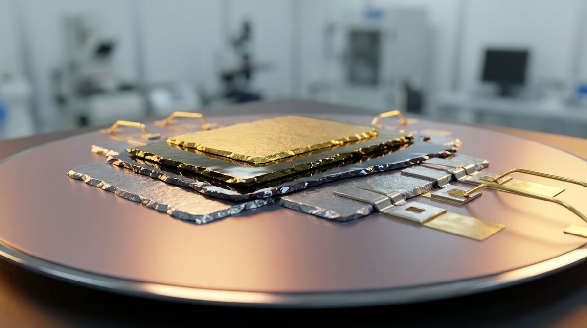
The device is a vertical stack consisting of a graphene channel gated by a MoS2/PtSe2 heterojunction. To build this, you will need high-quality 2D materials and precise transfer equipment.
Required Materials:
1. Graphene: High-quality CVD-grown graphene on a copper foil or a SiO2/Si substrate.
2. MoS2: Molybdenum disulfide, preferably CVD-grown for uniformity.
3. PtSe2: Platinum selenide, which provides the necessary band alignment for broadband absorption.
4. Substrate: Highly doped Silicon with a 300nm SiO2 layer to act as a back-gate.
5. Transfer Media: Polycarbonate (PC) or PMMA for dry transfer processes.
6. Contact Metal: Gold (Au) or Palladium (Pd) for high-performance ohmic contacts to the graphene.
Equipment Requirements:
1. An electron-beam evaporator or thermal evaporator for metal deposition.
2. A high-resolution optical microscope for alignment.
3. A dry transfer station (e.g., a polymer-assisted transfer setup) to stack the 2D layers.
4. A vacuum chamber to prevent contamination during the stacking process.
Building a van der Waals heterostructure requires extreme care to maintain the integrity of the interfaces. Any contamination between the MoS2 and PtSe2 layers will kill the photovoltaic effect.
Step 1: Substrate Preparation
Clean your SiO2/Si substrate using a standard RCA cleaning process or a piranha etch to ensure a pristine surface. This is critical for the graphene layer to adhere correctly.
Step 2: Graphene Deposition
If using CVD graphene, transfer the graphene onto the SiO2/Si substrate using a PMMA-assisted transfer method. Once transferred, bake the sample at approximately 150 degrees Celsius to remove residual polymer.
Step 3: Heterojunction Assembly (The Dry Transfer Method)
This is the most critical step. You should use a dry transfer method to avoid liquid solvents that can get trapped between layers.
1. Pick up a flake of MoS2 using a PC/PDMS stamp.
2. Position the MoS2 flake over the graphene channel.
3. Pick up a flake of PtSe2 using the same stamp.
4. Carefully stack the PtSe2 on top of the MoS2.
5. Press the stack onto the graphene channel.
6. Use a controlled heating element (around 100-150 degrees Celsius) to promote adhesion and squeeze out any micro-bubbles.
Step 4: Contact Formation
To measure the device, you must create electrical contacts. Use electron-beam evaporation to deposit metal electrodes (e.g., Au/Ti) onto the graphene. The contacts should be positioned such that they do not overlap the MoS2/PtSe2 heterojunction, as you want to measure the current flowing through the graphene channel under the influence of the heterojunction's gate effect.
Once the prototype is assembled, you must validate that it has overcome the gain-speed trade-off.
1. DC Characterization (I-V Curves): Perform current-voltage measurements in the dark and under illumination. You are looking for a significant change in the graphene channel current when light is applied. The ratio of the photocurrent to the dark current will give you the gain. Aim for a target of 10^6 to 10^8.
2. Transient Response (Speed Test): Use a pulsed laser source (e.g., a 405nm or 532nm laser) and a high-bandwidth oscilloscope (at least 1 GHz bandwidth). Measure the time it takes for the current to rise and fall. The target response time is below 550 ns.
3. Spectral Response: Use a broadband light source (visible to NIR) to confirm the device's sensitivity across different wavelengths. The MoS2/PtSe2 heterojunction should provide a broad response.
4. Detectivity Calculation: Use the measured responsivity and noise current to calculate the detectivity in Jones. The goal is to exceed 10^11 Jones.
Since this is a research-based prototype, several assumptions must be made for a lab implementation:
Assumption 1: Layer Thickness. The research does not specify the exact thickness of the MoS2 and PtSe2 flakes. For a practical prototype, assume starting thicknesses of 5-10 nm for each layer to ensure efficient charge separation while maintaining high absorption.
Assumption 2: Contact Resistance. We assume that the contact resistance between the metal and graphene is minimized through high-temperature annealing. If the resistance is too high, the device speed will be limited by the RC time constant rather than the carrier transit time.
Risk 1: Interfacial Contamination. The primary risk is the presence of hydrocarbons or water molecules between the MoS2 and PtSe2 layers. This will create traps that increase response time and decrease gain. A vacuum-based transfer process is highly recommended.
Risk 2: Material Uniformity. CVD-grown 2D materials can have grain boundaries. If the heterojunction is not continuous over the graphene channel, the device will exhibit inconsistent performance.
This guide is based on the research findings presented in:
Yin, Y., Zhang, J., Zhang, X., Zhang, J., Liu, L., Ma, H., Luo, X., & Gan, X. (2026). High-speed and high-gain graphene photovoltaic phototransistor gated by a van der Waals heterojunction. arXiv:2608.00771v1.
Serious about B2B integration? Test our premium Pulsed Electrical Resistive Carbon Heating turbostratic graphene in your lab. 100g sample packs available now.
Explore More
Researchers derived an analytic formula for twisted bilayer graphene electron lifetimes, providing a key design tool for future quantum and electronic devices.

Learn to build a high-responsivity 1.5 µm graphene photodetector. This guide details the materials and steps for a prototype based on upconversion...

New software for the modal analysis of electromagnetic resonators now includes 2D materials, accelerating the design of advanced graphene optical and...