
Modeling Graphene Resonators: New Software Unlocks Advanced Optical Design
New software for the modal analysis of electromagnetic resonators now includes 2D materials, accelerating the design of advanced graphene optical and...
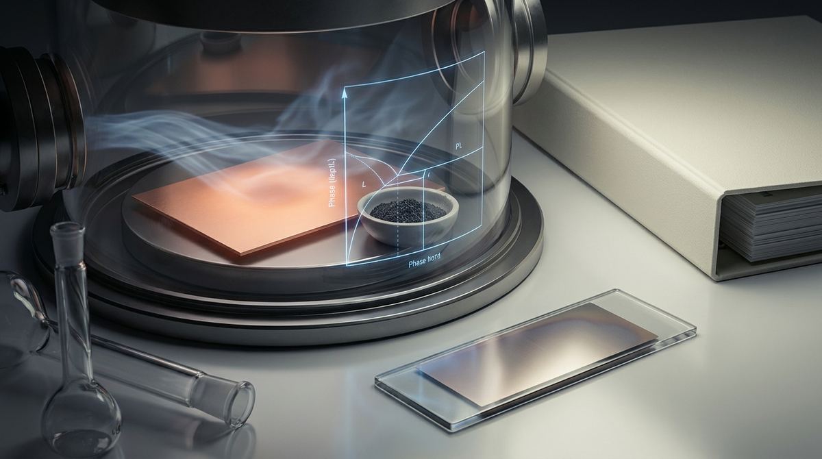
Imagine you are a master chef trying to bake the perfect soufflé. You know that if the oven is even five degrees too hot, the center collapses, and if it is slightly too cool, the texture becomes dense and gummy. For years, scientists trying to manufacture graphene—the world's thinnest, strongest material—have been facing this exact same problem. They have known that graphene can be grown on copper surfaces using a process called chemical vapor deposition, but they have struggled to make it happen perfectly every single time. Because the process is so sensitive to tiny changes in temperature and gas pressure, every batch of graphene can come out looking different. Some batches are perfect single layers, while others are a messy, multi-layered clump of carbon. This unpredictability has been a massive roadblock for moving graphene from a laboratory curiosity to a staple in the electronics we use every day.
The fundamental challenge in graphene manufacturing is the lack of a universal "recipe" that guarantees a consistent result. Currently, most chemical vapor deposition processes rely heavily on empirical testing, which is essentially a high-tech version of trial and error. If a company wants to grow a larger sheet of graphene or use a different type of gas, they often have to start the entire testing process from scratch to find the optimal settings. This is incredibly expensive and time-consuming. The core of the problem lies in the complex relationship between the carbon precursor gases, the thermal energy in the furnace, and the copper substrate itself.
When carbon atoms are deposited onto copper, they do not simply settle into a neat grid. They behave according to the laws of thermodynamics and kinetics, which are incredibly fickle. If the carbon atoms move too quickly across the copper surface, they might cluster together into unwanted thick patches instead of a smooth, single-atom layer. If they move too slowly, they might never form a continuous sheet, leaving holes in the material. Furthermore, the copper surface itself is not a perfect plane; it has grain boundaries and microscopic bumps that influence how the carbon lands and settles. Without a way to predict how these variables interact, engineers are essentially flying blind, attempting to scale up a process that is inherently chaotic.
To solve this, scientists need a map. In science, when we have a complex system with many moving parts, we create a phase diagram. You might have seen a phase diagram for water, which shows exactly which temperature and pressure will result in ice, liquid water, or steam. This research aims to create a similar map, but for graphene. Instead of showing ice and steam, this map shows the different "phases" of carbon growth on copper. It tells you, for any given temperature and any given gas pressure, whether you will end up with a single layer of beautiful graphene, a thick layer of graphite, or nothing at all.
By developing generalized phase diagrams, the researchers are moving away from specific, one-off recipes and moving toward a universal understanding of the growth process. Instead of saying, "Use this exact temperature for this specific machine," they are saying, "Under these thermodynamic conditions, this is the mathematical certainty of what will happen." This allows engineers to look at a target outcome—such as a perfectly uniform monolayer—and work backward to find the exact conditions needed to achieve it. It turns a guessing game into a predictable engineering discipline.
To understand how these phase diagrams are constructed, we must look at the mechanics of chemical vapor deposition on copper. The process typically begins by placing a copper foil into a furnace and filling it with a carbon-rich gas, such as methane. As the furnace reaches extremely high temperatures, the thermal energy causes the chemical bonds in the methane molecules to break apart. This leaves behind carbon atoms that land on the copper surface, while the hydrogen is swept away by the flow of gas.
The copper substrate plays a critical role because of its unique chemical properties. Unlike other metals like nickel, copper has a very low solubility for carbon at typical growth temperatures. This means that once the carbon atoms land on the copper, they do not sink deep into the metal; instead, they stay on the surface. This surface-mediated growth is what allows for the creation of single-layer graphene. As the carbon atoms land, they begin to collide and stick to one another through chemical bonds. This is where the physics gets complicated. The movement of these atoms, known as surface diffusion, is driven by the temperature. Higher temperatures give the atoms more kinetic energy, allowing them to move across the copper surface more easily to find their place in the hexagonal lattice.
The pressure of the gas also dictates the rate at which new carbon atoms arrive at the surface. If the pressure is high, the surface is bombarded with carbon atoms, which can lead to rapid, uncontrolled growth. If the pressure is low, the arrival rate is slower, allowing more time for the atoms to organize themselves into a perfect structure. The phase diagram captures the intersection of these two forces—the rate of carbon arrival and the speed of carbon movement—to define the boundaries of successful growth.
In this study, Tongtong Wang, Ke Jin, Yishi Zhang, and Dajun Shu have provided a mathematical framework that maps out these complex interactions. By analyzing how the chemical potential of carbon changes under different environmental conditions, they have identified the boundaries that separate different growth modes. Their work moves beyond simple observations and provides a generalized model that can account for various growth scenarios on copper.
One of the most significant findings involves the transition between different types of growth. The researchers were able to identify the specific thresholds where the system shifts from producing a continuous, high-quality monolayer to producing fragmented islands or multi-layered graphite. By defining these boundaries, the research provides a way to navigate the "growth landscape." For example, the researchers can now predict how a change in the carbon-to-hydrogen ratio will affect the nucleation density—the number of points where the graphene starts to grow. Understanding this density is vital because if too many nuclei form at once, the graphene sheets will collide and create many defects and wrinkles; if too few form, the graphene will be full of empty gaps.
The ability to predict graphene growth through phase diagrams is a massive leap forward for industrial scalability. In any manufacturing industry, the goal is "repeatability." If you are making microchips, you need every single chip to behave exactly the same way. Current graphene production often lacks this level of control, which is why we do not see graphene in every smartphone or computer yet. By providing a map that predicts outcomes, this research allows manufacturers to design automated systems that can adjust temperature and pressure in real-time to maintain perfect growth conditions.
Furthermore, this research provides a foundation for material optimization. If a company wants to grow graphene on a different type of copper alloy, or if they want to use a different precursor gas to save costs, they no longer have to start from zero. They can use the principles established in these generalized phase diagrams to predict the behavior of the new system. This drastically reduces the research and development costs associated with new material applications. It essentially provides a shortcut for the entire scientific community, allowing them to jump straight to the most promising growth conditions.
While this work is a significant advancement, it is important to recognize that a theoretical or modeled phase diagram is not a magic wand. One of the primary limitations is that these models often assume an "ideal" copper surface. In a real-world factory, copper foils have impurities, surface roughness, and varying crystal orientations that can disrupt the predicted growth patterns. A phase diagram might say that a certain temperature will produce a perfect layer, but a single microscopic grain boundary in the copper could cause a defect in the graphene.
Additionally, the scale of the testing is a factor. Most detailed studies of graphene growth are performed on small, laboratory-scale samples. Scaling this up to "roll-to-roll" manufacturing—where massive sheets of copper are continuously pulled through a furnace—introduces complex fluid dynamics and thermal gradients that are much harder to model than a static piece of foil. Future research will need to integrate these generalized phase diagrams with more complex models of large-scale industrial machinery to ensure that the "map" still works when applied to a massive production line.
The implications for real-world technology are vast. In the realm of electronics, high-quality, uniform graphene is essential for the development of high-speed transistors and flexible displays. Because graphene is incredibly conductive and transparent, it could lead to the next generation of foldable smartphones and wearable sensors that are more responsive and durable than current silicon-based tech.
In the energy sector, graphene is a candidate for revolutionizing battery technology. By using graphene-enhanced electrodes, batteries could charge much faster and last through more charge cycles. The ability to grow large, defect-free sheets of graphene through predictable CVD processes is the key to making these advanced batteries commercially viable. We also see potential in water filtration systems, where graphene membranes can be used to filter salt and contaminants from water at a molecular level, and in aerospace, where graphene-reinforced composites could make aircraft lighter and stronger.
If you take away only one idea from this research, let it be this: the transition from laboratory science to industrial manufacturing requires moving from "trial-and-error" to "predictable control," and generalized phase diagrams are the essential maps that make that transition possible for graphene.
How does copper help grow graphene?
Copper acts as a catalyst that breaks down the carbon-containing gas into individual carbon atoms. Because copper does not absorb carbon easily, it forces the carbon to stay on the surface, which helps form a thin, single-atom layer of graphene rather than a thick chunk of graphite.
What is a phase diagram in simple terms?
A phase diagram is a visual map that shows the state of a substance under different conditions. For example, it shows exactly how much heat or pressure is needed to turn water into ice or steam. In this research, the map shows the conditions needed to grow perfect graphene.
Why is it so hard to grow graphene consistently?
Graphene growth is extremely sensitive to tiny changes. Small fluctuations in temperature or the amount of gas can change the result from a perfect layer to a messy, useless clump. This unpredictability makes it difficult for factories to produce consistent materials.
What is the difference between monolayer and multilayer graphene?
Monolayer graphene is a single layer of atoms, which is the ideal form for most high-tech electronics because it is extremely thin and highly conductive. Multilayer graphene is many layers thick, which changes its electrical and physical properties and is often undesirable for high-performance applications.
Will this research lead to graphene-powered devices immediately?
Not immediately. While this research provides the "map" needed for better manufacturing, there is still work to do in scaling these processes up to large industrial sizes and managing real-world impurities in the materials used. It is a critical step toward that future, however.
The journey of graphene from a scientific marvel to a commercial powerhouse has been defined by the struggle for control. The work of Tongtong Wang, Ke Jin, Yishi Zhang, and Dajun Shu provides a vital piece of that puzzle. By creating generalized phase diagrams for CVD growth on copper, they have provided the scientific community with a way to predict and control the chaotic nature of carbon deposition. This move toward a predictive, rather than empirical, model is exactly what is required to turn the promise of graphene into a reality for the electronics, energy, and environmental industries. As we refine these models and move toward large-scale implementation, the era of predictable, high-quality graphene manufacturing is clearly on the horizon.
Serious about B2B integration? Test our premium Pulsed Electrical Resistive Carbon Heating turbostratic graphene in your lab. 100g sample packs available now.
Explore More
New software for the modal analysis of electromagnetic resonators now includes 2D materials, accelerating the design of advanced graphene optical and...

New research provides a theoretical framework for calculating the lifetime and spectral function of topological heavy fermions, a key step for developing...

Learn to build a prototype strain-tunable magnetic device using graphene as a sacrificial layer to create freestanding MnPtGa membranes. This guide covers...