
Understanding the Lifetime of Topological Heavy Fermions in Graphene Systems
New research provides a theoretical framework for calculating the lifetime and spectral function of topological heavy fermions, a key step for developing...
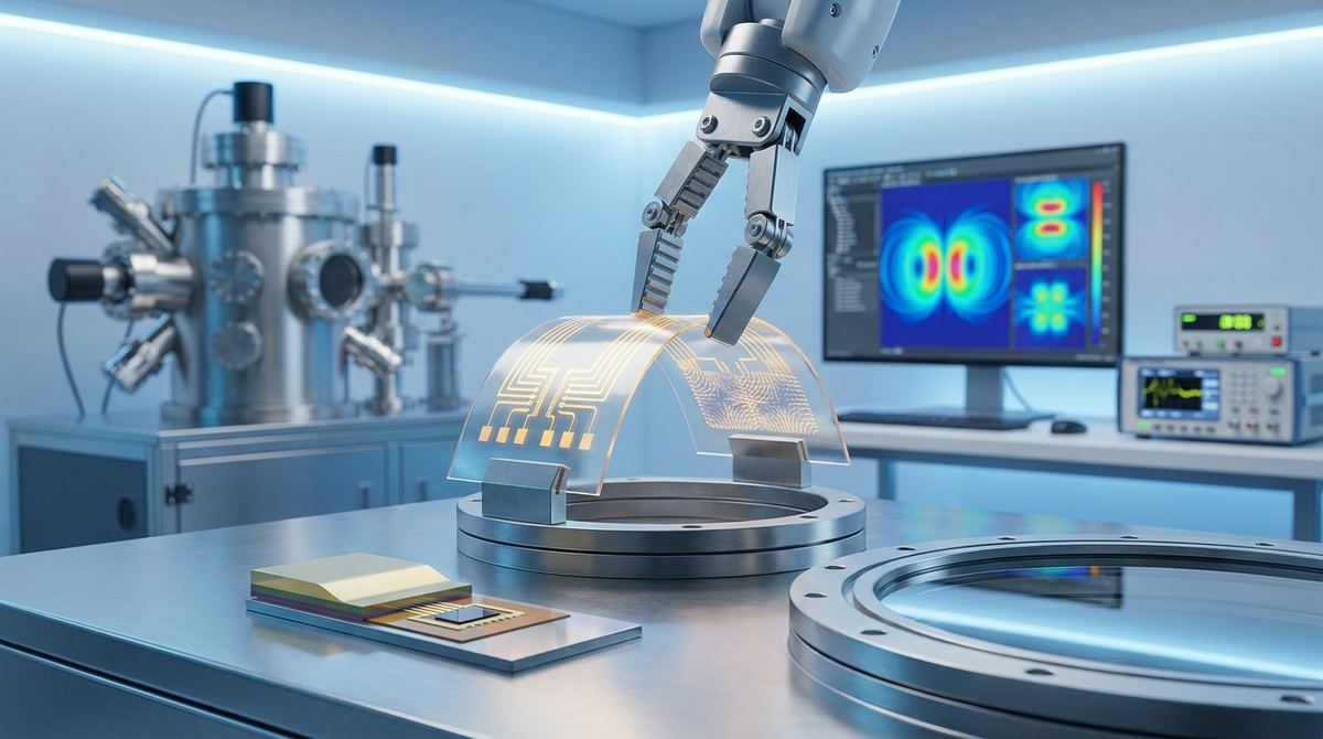
For decades, the foundation of computing has been the electron's charge. A transistor is either on or off, a bit is a one or a zero, based on the presence or absence of a group of electrons. While this binary system has been incredibly successful, it is approaching fundamental limits in power consumption and heat generation. This has driven researchers to explore alternative properties of the electron, most notably its spin.
Spintronics, or spin electronics, aims to build devices that operate based on the electron's magnetic moment, or spin. This opens the door to technologies like magnetic random-access memory (MRAM) that are non-volatile, faster, and more energy-efficient. The next frontier in this field is straintronics: the active control of these magnetic states not with magnetic fields or electrical currents, but with mechanical strain. Imagine a memory bit that is written by physically flexing the material, or a logic gate that switches with a nanomechanical impulse. This would represent a paradigm shift in low-power computing.
The primary challenge has been a practical one. To apply meaningful strain to a crystalline material, it must be freestanding or on a flexible substrate. However, the highest quality crystalline films are grown on rigid, single-crystal wafers in a process called epitaxy. The film is locked to the wafer, making it impossible to bend or stretch.
This is where graphene provides an elegant solution. By growing the desired crystalline material on top of a graphene layer that has been placed on a conventional wafer, we can have the best of both worlds. The graphene acts as a template for high-quality crystal growth but forms only weak van der Waals bonds with the film above it. This allows the newly grown film to be peeled off mechanically, creating a perfect, freestanding crystalline membrane.
A recent paper by R. Rawat et al. demonstrates this exact principle with a fascinating material, Manganese-Platinum-Gallium (MnPtGa). They show that by growing it on graphene, they can create freestanding membranes and then alter the material's magnetic state by physically rippling it. This guide translates their breakthrough into a practical project for an ambitious lab or startup: building a prototype strain-tunable magnetic device.
Our objective is to construct and test a device that demonstrates the core principle of straintronics. The prototype will consist of a thin, freestanding membrane of single-crystal MnPtGa, transferred from its growth substrate to a flexible backing. This membrane will be integrated into a test fixture that allows for the application of controlled mechanical bending.
The success of the project will be determined by our ability to measure a change in the material's physical properties in response to this applied strain. While the source research used sophisticated magnetic and optical measurements, we will adapt the test plan for a more accessible approach using electrical resistance measurements. The goal is to observe a clear, repeatable change in the material's electrical behavior at low temperatures when it is mechanically flexed, confirming that we are, in fact, tuning its internal magnetic order with strain.
This project involves advanced material synthesis and characterization. Access to specialized facilities, either in-house or through academic or commercial partnerships, is essential.
Materials and Chemicals:
Substrates: 4-inch Germanium (111)-oriented single-crystal wafers.
Graphene Source: High-quality, single-layer CVD graphene grown on copper foil.
Flexible Substrate: Polyimide (Kapton) or PET film, approximately 50-100 micrometers thick.
Deposition Targets: High-purity (99.99% or better) elemental sources of Manganese (Mn), Platinum (Pt), and Gallium (Ga) for molecular beam epitaxy.
Process Chemicals: Acetone, isopropyl alcohol, deionized water, photoresist and developer for lithography, PMMA (Poly(methyl methacrylate)) for graphene transfer, and an etchant for copper (e.g., ammonium persulfate).
Contacts: Gold (Au) and a thin adhesion layer like Titanium (Ti) or Chromium (Cr) for electrical contacts.
Equipment:
Film Growth: A molecular beam epitaxy (MBE) system is required for growing the single-crystal MnPtGa film. This is the most critical piece of equipment.
Graphene Synthesis and Transfer: A CVD tube furnace is needed if growing graphene in-house. For those looking to build this capability, various forms of graphene production machinery are available. Otherwise, standard wet bench facilities are needed for the transfer process.
Patterning: Photolithography or e-beam lithography equipment to define electrical contacts. A metal evaporator (e-beam or thermal) is needed for depositing the contacts.
Assembly: A wire bonder for connecting the device to a chip carrier. Micromanipulators and a high-resolution optical microscope are essential for handling the delicate membranes.
Test and Measurement:
A cryostat or probe station capable of reaching temperatures down to at least 77 K (liquid nitrogen temperature).
A temperature controller.
A precision source measure unit (SMU) or a combination of a current source and nanovoltmeter for four-point probe resistance measurements.
A custom-built two-point or four-point bending jig to apply strain.
The fabrication process is a multi-stage procedure requiring precision and patience, especially during the membrane transfer step.
1. Substrate Preparation: The Graphene Release Layer
The process begins by creating the graphene-on-germanium substrate.
Start with a clean Ge(111) wafer. Perform a standard solvent clean (acetone, IPA) followed by a deionized water rinse and nitrogen blow-dry.
Take your CVD graphene on copper foil. Spin-coat a layer of PMMA on top of the graphene.
Etch away the copper foil using your chosen etchant, leaving the PMMA/graphene film floating.
Carefully transfer the floating film to a bath of deionized water to rinse away etchant residue. Repeat this several times.
"Fish" the PMMA/graphene film out of the water using the clean Ge(111) wafer.
Allow the stack to dry completely, then bake at a moderate temperature (e.g., 150-180°C) to improve adhesion.
Finally, remove the PMMA scaffold by dissolving it in acetone, leaving a single layer of graphene on the Ge(111) wafer.
2. MnPtGa Crystalline Film Growth
This step requires an MBE system and is the most research-intensive part of the process. The source paper confirms successful growth but does not provide a detailed recipe. The following are engineering assumptions for a starting point.
Load the graphene/Ge(111) substrate into the MBE chamber.
Outgas the substrate at high temperature to ensure an atomically clean surface.
Engineering Assumption: The optimal growth temperature for MnPtGa on graphene is not specified. A reasonable starting range to explore would be 300°C to 500°C.
Co-deposit Mn, Pt, and Ga from effusion cells onto the heated substrate. The relative flux rates must be carefully calibrated to achieve the desired 1:1:1 stoichiometry of the MnPtGa crystal.
Engineering Assumption: The target film thickness should be in the range of 20-50 nm. This is thin enough to be flexible but thick enough to maintain its crystalline properties and provide a measurable electrical signal.
The growth process must be monitored in-situ using techniques like RHEED (Reflection High-Energy Electron Diffraction) to confirm that single-crystal epitaxial growth is occurring. This is a critical step for creating the high-quality films needed for these advanced graphene electronics.
3. Membrane Release and Device Transfer
This is the step where graphene's unique properties are leveraged.
First, pattern the flexible Kapton substrate. Use photolithography and metal evaporation to create gold contact pads and traces where your device will eventually sit.
To release the membrane, you can use a thermal release tape or a polymer stamp (like PDMS) as an intermediate carrier. Press the carrier firmly and evenly onto the surface of the MnPtGa film.
Carefully and slowly peel the carrier away from the Ge wafer. The weak van der Waals forces between the MnPtGa and the graphene will give way, allowing the MnPtGa film (and likely the graphene layer as well) to be lifted off the rigid substrate. You now have a freestanding crystalline membrane on a temporary carrier.
Align this carrier with the pre-patterned Kapton substrate under a microscope and gently press it down.
If using thermal release tape, a gentle heating will release the membrane onto the Kapton. If using a PDMS stamp, the differential adhesion will favor the bond to the Kapton, allowing the stamp to be peeled away, leaving the membrane behind.
4. Final Device Integration
If contacts were not pre-patterned on the Kapton, you must now use a shadow mask or lithography to define and deposit Ti/Au contacts directly onto the transferred membrane. This is more challenging due to the fragility of the film.
Mount the flexible Kapton substrate into your custom bending jig.
Use a wire bonder to connect the gold pads on the Kapton to a chip carrier for easy connection to the measurement electronics.
The test plan aims to replicate the core finding of the source paper—mechanical control of the magnetic state—using an electrical resistance measurement as a proxy.
1. Baseline Measurement (Unstrained)
Place the device, mounted in its jig but in a flat, unstrained state, into the cryostat.
Connect the four-point probe contacts to your SMU.
Cool the device down from room temperature to 77 K while continuously measuring its resistance. Record resistance as a function of temperature.
The source paper identifies a magnetic anomaly around 140 K. Engineering Assumption: We expect to see a corresponding feature in our electrical data. This might be a "kink" or a distinct change in the slope (dR/dT) of the resistance-temperature curve around 140 K. This is because magnetic ordering transitions often alter electron scattering rates, which directly impacts resistivity.
2. Strained Measurement
Actuate the bending jig to apply a known, uniform curvature to the Kapton substrate and the MnPtGa membrane. A moderate strain of 0.1% to 0.5% is a good target.
While holding the device in this strained configuration, repeat the exact same temperature sweep from room temperature down to 77 K, again recording resistance versus temperature.
3. Data Analysis and Confirmation
Plot the two resistance-temperature curves (strained and unstrained) on the same graph.
Also, plot the derivative (dR/dT) for both curves. This can make subtle changes in slope much more apparent.
Expected Result: Based on the paper's conclusion that rippling "suppresses the ~140 K magnetic anomaly," we expect the feature we identified at 140 K in the unstrained device to be significantly diminished, shifted to a different temperature, or to disappear entirely in the strained measurement.
Observing this change would be a successful demonstration of the prototype. It would show that you have mechanically altered the electronic and magnetic ground state of the material, which could form the basis for novel sensors or memory elements. This principle is a key driver for developing new types of graphene sensors.
This is an advanced project with significant challenges. Acknowledging them is key to success.
Equipment Access: An MBE system is a multi-million dollar piece of equipment and is the largest barrier to entry. Mitigation: Seek collaboration with a university that has a materials science department or user facility. Alternatively, explore services from commercial epitaxial growth foundries.
Membrane Integrity: The MnPtGa membranes are nanometers thick and extremely fragile. They can easily tear or crack during the transfer process. Mitigation: This requires practice. Use of automated or semi-automated stamp transfer systems can improve yield. Work slowly and methodically under a microscope.
Indirect Measurement: Using resistance as a proxy for magnetic order is a valid but indirect method. The underlying physics connecting the two can be complex. Mitigation: For this prototype, a clear and repeatable change in the electrical signal correlated with strain is sufficient proof-of-concept. For further research, the results should be validated against direct magnetic measurements like SQUID or magneto-optical Kerr effect (MOKE) magnetometry.
Growth Calibration: Achieving high-quality, single-crystal MnPtGa requires significant process development. Mitigation: Budget ample time for MBE calibration runs. Use surface science tools like XRD and AFM to characterize your films before attempting the difficult transfer step.
This practical guide is an engineering interpretation based on the foundational research presented by R. Rawat et al. in their 2026 paper, "Mechanical control of competing magnetic order in crystalline MnPtGa membranes." The core technique of using graphene as a release layer to create freestanding, strain-tunable MnPtGa membranes is taken directly from their work. Our proposed device architecture and electrical test plan are practical adaptations designed to make the concept accessible for prototype development in a small lab or startup environment.
The long-term potential for this technology is immense. Devices that can be controlled by mechanical stress instead of electrical current could lead to dramatic reductions in power consumption for data storage and logic. This could unlock new computing architectures, especially for edge computing and IoT where power is at a premium. While significant engineering hurdles remain, the fusion of advanced magnetic materials with graphene's unique mechanical properties charts a clear path forward. For those tracking the commercial viability of such innovations, ongoing graphene market research will be crucial in identifying when these laboratory breakthroughs are ready to transition into industrial applications.
Serious about B2B integration? Test our premium Pulsed Electrical Resistive Carbon Heating turbostratic graphene in your lab. 100g sample packs available now.
Explore More
New research provides a theoretical framework for calculating the lifetime and spectral function of topological heavy fermions, a key step for developing...

Researchers revisit a graphene, n-heptane, and permalloy system, observing apparent ideal diamagnetism at ambient conditions, a key property of superconductors.

Researchers are using artificial intelligence to autonomously discover optimal recipes for growing graphene, a breakthrough in AI-driven graphene synthesis...