
Nature's Nanotech: Graphene and Blue Emission Found in Bee Hives
Researchers discover naturally formed graphene sheets and carbon ovals in stingless bee hives, creating a novel emergent material with powerful blue light...
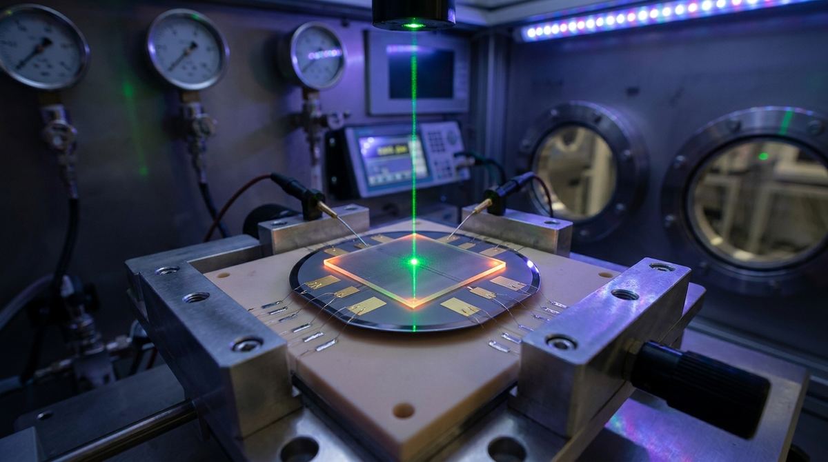
For years, the primary challenge in graphene-based electronics was the transition from laboratory-scale exfoliated flakes to industrial-scale production. Exfoliated graphene is excellent for proof-of-concept, but it is impossible to scale for mass-market sensors. Chemical Vapor Deposition (CVD) graphene solves this by allowing for large-area, uniform films that can be transferred onto various substrates.
This guide focuses on a specific, highly practical application: the construction of high-sensitivity photodetectors using CVD graphene on a Silicon/Silicon Dioxide (Si/SiO2) substrate. Instead of relying on the intrinsic carrier transport of graphene alone, we utilize a mechanism known as photogating. This approach allows for extremely high sensitivity, making it ideal for low-light detection, industrial light sensing, and specialized lab equipment.
To build these devices, you must understand the physics that drives the signal. In a graphene/SiO2/Si structure, the device acts as a field-effect transistor (FET) where the Si substrate acts as a back-gate.
When light with energy higher than the Silicon bandgap (wavelengths shorter than approximately 1100 nm) hits the substrate, it generates electron-hole pairs within the Silicon. Some of these carriers become trapped at the Si/SiO2 interface. These trapped charges act as a local, permanent gate voltage that shifts the Fermi level of the graphene layer. This shift changes the graphene's resistance, resulting in a measurable change in current.
Because the trapped charges are not immediately neutralized, this mechanism provides a significant amplification effect, leading to very high sensitivity. However, engineers should note that because this relies on charge trapping, these devices are generally not suitable for high-frequency telecom applications where extremely fast response times are required.
To prototype this device, you will need the following materials and tools. Note that some specific parameters are engineering assumptions based on standard cleanroom practices.
Materials:
- CVD Graphene: Monolayer, bilayer, or trilayer graphene grown on copper foil.
- Substrate: Silicon wafers with a 285 nm or 300 nm thermal SiO2 layer.
- Metal for Contacts: Chromium (Cr) and Gold (Au) or Titanium (Ti) and Gold (Au) for high-conductivity, low-resistance contacts.
- Transfer Polymer: Poly-methyl methacrylate (PMMA).
- Etchants: Copper etchant (e.g., Ammonium Persulfate) and PMMA remover (Acetone).
- Cleaning Agents: Isopropanol (IPA) and Deionized (DI) water.
Equipment:
- Photolithography system (Mask aligner and photoresist coater).
- Thermal evaporator or Sputter coater for metal deposition.
- Vacuum annealing furnace.
- Optical microscope and Scanning Electron Microscope (SEM) for inspection.
- Probe station for electrical characterization.
The research indicates a critical fabrication detail: the order of operations between metal contact deposition and graphene transfer determines the device performance. To achieve the highest photoresponse, you must fabricate your metal contacts on the substrate before you transfer the graphene.
1. Substrate Preparation: Clean the Si/SiO2 substrate using a standard RCA clean or a simple sonication in IPA and DI water to remove organic contaminants.
2. Contact Patterning:
- Apply a layer of photoresist via spin-coating.
- Use photolithography to define the contact pads.
- Deposit the metal layers (e.g., 5 nm Cr/Ti followed by 50 nm Au) using thermal evaporation.
- Perform lift-off in a solvent to leave clean, patterned metal pads on the SiO2 surface.
3. Graphene Transfer:
- Prepare the CVD graphene on its growth substrate (Copper).
- Coat the graphene with PMMA.
- Etch the copper layer using an etchant solution.
- Carefully transfer the PMMA/Graphene film onto the patterned Si/SiO2 substrate.
- Ensure the graphene layer overlaps the pre-fabricated metal contacts.
4. Polymer Removal and Annealing:
- Rinse the sample in Acetone to remove the PMMA.
- Perform a post-transfer anneal in a vacuum furnace.
- Assumption: A temperature range of 200C to 300C for 1 to 3 hours is recommended to remove residual polymer and improve contact resistance.
One of the most important engineering decisions is deciding how many layers of graphene to use. The research shows a clear trade-off between sensitivity and noise.
Monolayer Graphene:
- Use this if your primary goal is maximum sensitivity.
- The research reports a sensitivity as high as 995 A/W for monolayer CVD graphene.
- The thinness of the monolayer allows for maximum modulation of the carrier density by the photogating effect.
Bilayer or Trilayer Graphene:
- Use this if you need higher detectivity (the ability to distinguish a signal from background noise).
- As you add layers, the sensitivity decreases due to two factors: screening (the outer layers shield the inner layers from the electric field) and parallel conduction (the extra layers provide more paths for current, diluting the relative change in resistance).
- However, the additional layers can lower the overall noise level of the device, potentially resulting in a better signal-to-noise ratio for specific applications.
Once the prototype is fabricated, follow this testing plan to validate the device.
1. Dark Current Measurement: Place the device in a light-proof environment and measure the current-voltage (I-V) characteristics. This establishes your baseline resistance.
2. Photoresponse Measurement:
- Use a calibrated light source (e.g., a 532 nm laser or a white LED with a specific wavelength filter).
- Measure the I-V curves under illumination.
- Calculate the change in current (Delta I) caused by the light.
3. Sensitivity Calculation:
- Calculate the Responsivity (R) using the formula: R = Delta I / P, where P is the incident optical power (W).
- Compare your results against the 995 A/W benchmark for monolayer devices.
4. Gate-Voltage Dependence:
- Use the Si substrate as a back-gate.
- Sweep the gate voltage and observe how the photoresponse changes. This confirms the photogating mechanism and helps you identify the optimal operating voltage for your specific application.
- Residue Contamination: The most common failure point is PMMA residue left on the graphene surface after transfer. This significantly increases contact resistance and decreases sensitivity.
- Mitigation: Use a high-purity acetone rinse and ensure the vacuum annealing step is performed thoroughly.
- Graphene Cracking: During the transfer process, graphene can develop micro-cracks, especially if the transfer speed is inconsistent.
- Mitigation: Use a controlled, slow transfer process and inspect the surface via SEM to ensure continuity.
- Contact Resistance: If the metal contacts do not make intimate contact with the graphene, the signal will be lost.
- Mitigation: Always follow the contact-first fabrication method as suggested by the research to ensure the graphene is pressed directly onto the metal pads during transfer.
This guide is based on the research findings of Matienko, Borisenko, and Kuntsevich (2026) regarding large-area CVD graphene photogating.
The following are engineering assumptions provided for practical implementation:
- Annealing temperatures (200C-300C) are standard industry values for PMMA removal and are not explicitly detailed in the source.
- Metal thicknesses (5nm/50nm) are standard values for high-conductivity contact pads.
- The light source wavelength (visible spectrum) is assumed based on the source's mention of photon energies above the Silicon bandgap.
- The sensitivity value of 995 A/W is a benchmark from the source for monolayer graphene and serves as a target for your prototype.
Serious about B2B integration? Test our premium Pulsed Electrical Resistive Carbon Heating turbostratic graphene in your lab. 100g sample packs available now.
Explore More
Researchers discover naturally formed graphene sheets and carbon ovals in stingless bee hives, creating a novel emergent material with powerful blue light...

Discover how rippled graphene pores act as fluidic memristors, enabling advanced synaptic functionalities for the next generation of neuromorphic computing.

Learn how to use electromechanical responses in gapped graphene to measure electronic temperature and band gaps using traveling flexural waves.