
Nature's Nanotech: Graphene and Blue Emission Found in Bee Hives
Researchers discover naturally formed graphene sheets and carbon ovals in stingless bee hives, creating a novel emergent material with powerful blue light...
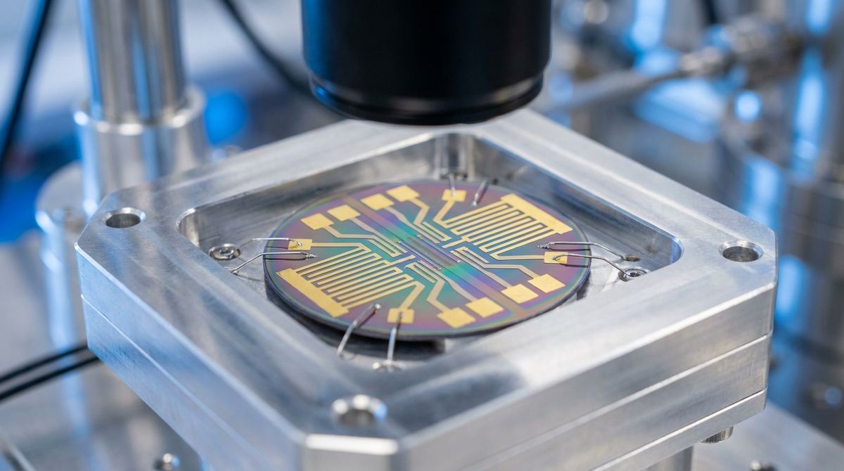
As artificial intelligence models scale toward trillions of parameters, the bottleneck in computing performance is shifting from raw processing power to data movement. The interconnects between chips, memory, and storage must handle massive bandwidth with minimal latency and power consumption. Optical interconnects are the primary candidate to solve this, but traditional semiconductor-based photodetectors often struggle to balance speed and sensitivity.
Graphene has long been touted as the ideal material for these optical receivers because it is inherently broadband and can operate at extremely high speeds. However, graphene photodetectors face a fundamental engineering hurdle: the responsivity-bandwidth trade-off. In standard graphene devices, the carriers absorb light and become hot, but they lose that energy through rapid cooling to the substrate. This rapid cooling limits the responsivity (the electrical signal produced per unit of light), while attempting to increase sensitivity often slows down the device.
To build a high-performance 160 Gbps receiver, you must move beyond simple graphene-on-silicon architectures and move toward heterostructure engineering.
The research by Soundarapandian et al. demonstrates that you can break the responsivity-bandwidth trade-off by modifying the dielectric environment. Instead of placing graphene directly on a standard substrate like SiO2, you encapsulate the graphene between layers of Tungsten Diselenide (WSe2).
This WSe2 encapsulation architecture serves a critical purpose: it suppresses out-of-plane energy dissipation. By surrounding the graphene with WSe2, you increase the cooling length of the hot carriers to approximately 2.68 micrometers and reduce the heat-exchange coefficient. This allows the carriers to remain in a high-energy state longer, significantly boosting the responsivity without sacrificing the ultrafast response times required for high-speed data.
For an engineer, this means you can achieve a zero-bias photodetector—meaning no external voltage is required to drive the signal—which drastically reduces power consumption in high-density AI data centers.
To prototype this device, you will need access to a cleanroom environment and the following materials:
1. High-quality CVD Graphene: Ideally, a single layer of high-mobility graphene.
2. WSe2 Flakes or CVD Film: Used for the top and bottom encapsulation layers.
3. Substrate: Silicon with a thick thermal oxide layer (SiO2/Si) for electrical isolation.
4. Contact Metals: Titanium (Ti) for adhesion and Gold (Au) for high conductivity.
5. Etching Chemicals: Reactive Ion Etching (RIE) gases (such as CF4 or SF6) for patterning.
6. Transfer Medium: PDMS (Polydimethylsiloxane) or PC (Polycarbonate) for dry transfer of 2D materials.
7. Light Source: A C-band (1550 nm) tunable laser for testing.
8. Measurement Equipment: A high-speed oscilloscope (at least 50-100 GHz bandwidth) and a Bit Error Rate Tester (BERT).
Building a WSe2/Graphene/WSe2 heterostructure requires precise control over the transfer process to avoid contamination or wrinkles.
1. Substrate Preparation: Clean the SiO2/Si substrate using standard RCA cleaning or oxygen plasma to ensure a pristine surface.
2. Bottom Layer Transfer: Using a dry transfer method with a PDMS stamp, pick up a high-quality WSe2 flake and lay it onto the substrate. This layer acts as the bottom dielectric/encapsulation.
3. Graphene Transfer: Pick up a single layer of CVD graphene and transfer it directly onto the WSe2 layer. Ensure the alignment is precise to minimize strain.
4. Top Layer Transfer: Pick up a second WSe2 flake and encapsulate the graphene. This sandwich structure (WSe2/Graphene/WSe2) is the core of the device.
5. Photolithography and Contact Patterning: Use electron-beam lithography or high-resolution photolithography to define the contact areas.
6. Metal Deposition: Deposit a thin layer of Titanium (approx. 5-10 nm) followed by a thicker layer of Gold (approx. 50-100 nm) via electron-beam evaporation.
7. Etching: Use Reactive Ion Etching to define the active channel area and remove excess metal and material, leaving only the contact pads and the encapsulated channel.
Once fabricated, the device must be validated against the performance metrics established in the research.
1. DC Responsivity Test: Using a C-band laser, measure the photocurrent produced at zero bias. The goal is to reach a responsivity of approximately 0.12 A/W. If the value is significantly lower, check for interface contamination between the WSe2 and graphene.
2. Frequency Response: Use a vector network analyzer or a high-speed oscilloscope to measure the S-parameters. The device should maintain a flat response up to at least 110 GHz.
3. Data Rate Verification: This is the most critical test for AI applications. Use a Bit Error Rate Tester (BERT) to drive the device with NRZ (Non-Return-to-Zero) signals at 120 Gbps or PAM-4 (Pulse Amplitude Modulation) signals at 160 Gbps.
4. Eye Diagram Analysis: Observe the eye diagram on the oscilloscope. A clean, open eye at 160 Gbps PAM-4 indicates that the heterostructure engineering has successfully mitigated the trade-off between speed and signal integrity.
Since this is a guide for prototyping, several parameters must be assumed based on standard microfabrication practices:
- Channel Dimensions: For high-speed operation, the graphene channel length should be kept small, likely between 10 and 20 micrometers, with a width of 5 to 10 micrometers.
- Temperature: Tests should be conducted at room temperature (approx. 293 K), though thermal management during high-power laser testing is vital.
- Laser Wavelength: All optical testing is assumed to be in the C-band (centered around 1550 nm).
- Contact Resistance: It is assumed that the Ti/Au contacts will achieve low contact resistance through optimized annealing, though the exact temperature for annealing is not specified and should be tested cautiously between 200 and 300 degrees Celsius.
1. Interface Contamination: The biggest risk in 2D heterostructures is trapped air or polymer residue between the layers. This will kill the responsivity. Mitigation: Use a vacuum-based dry transfer method and perform a mild vacuum anneal after assembly.
2. Mechanical Strain: Wrinkles in the WSe2 or graphene can create local electric field variations. Mitigation: Control the transfer speed and temperature during the stacking process.
3. Contact Resistance: High contact resistance will limit the bandwidth. Mitigation: Optimize the metal deposition parameters and consider a post-deposition thermal anneal to improve the metal-graphene interface.
4. Thermal Management: While the WSe2 helps with carrier cooling, excessive laser power can still cause local heating. Mitigation: Always start with low optical power and increase incrementally while monitoring the DC responsivity.
This guide is based on the research findings presented in:
Pandian Soundarapandian, K., et al. (2026). C-band 160 Gbs-1 Zero-bias Graphene Photodetectors: Breaking the Responsivity-Bandwidth Trade-off by Heterostructure Engineering. arXiv:2605.23627v1.
Serious about B2B integration? Test our premium Pulsed Electrical Resistive Carbon Heating turbostratic graphene in your lab. 100g sample packs available now.
Explore More
Researchers discover naturally formed graphene sheets and carbon ovals in stingless bee hives, creating a novel emergent material with powerful blue light...

Discover how rippled graphene pores act as fluidic memristors, enabling advanced synaptic functionalities for the next generation of neuromorphic computing.

Learn how to use electromechanical responses in gapped graphene to measure electronic temperature and band gaps using traveling flexural waves.