
Nature's Nanotech: Graphene and Blue Emission Found in Bee Hives
Researchers discover naturally formed graphene sheets and carbon ovals in stingless bee hives, creating a novel emergent material with powerful blue light...
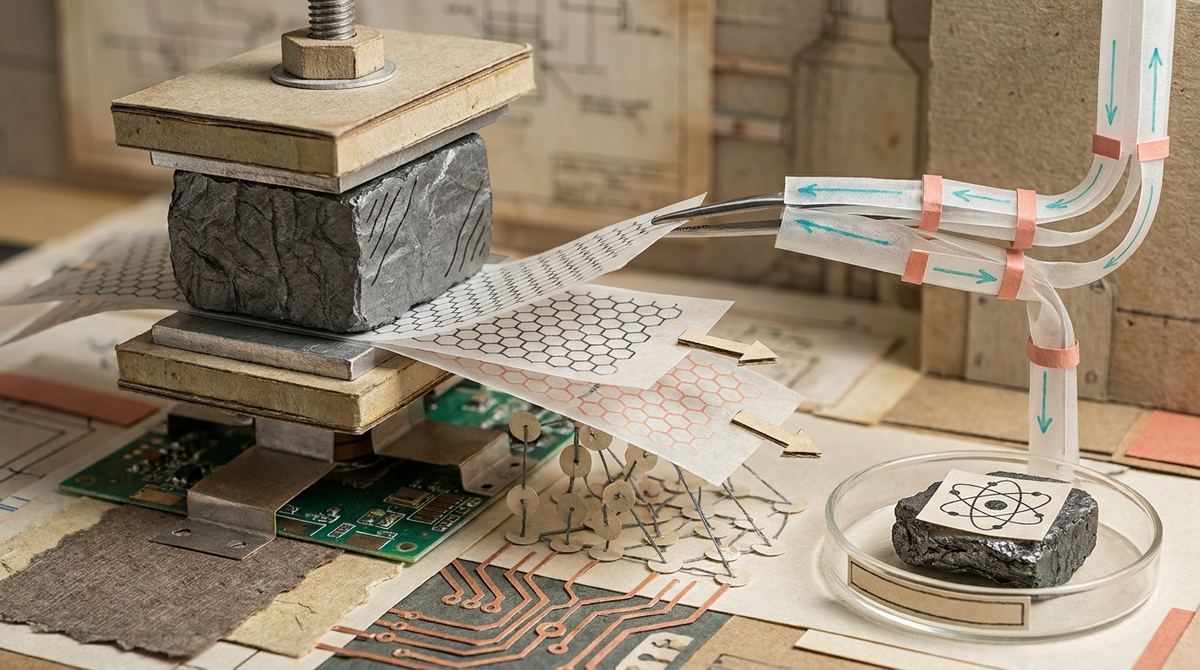
Imagine a computer memory chip that is so small it is measured in atoms, yet so efficient that it requires almost no energy to switch between a zero and a one. Traditional electronics rely on moving large groups of electrons or shifting ions within a bulky solid, a process that generates heat and limits how small we can make our devices. However, a new frontier of physics suggests we can achieve this by simply sliding one thin sheet of material over another. This research into the movement of atomic layers offers a glimpse into a future where electronics are faster, smaller, and far more sustainable.
In a detailed investigation into the complexities of these atomic movements, researchers Sourav Paul, Prasenjit Ghosh, Krishna Prasad Maity, Vineet Pandey, Abhijith M. B., Premananda Chatterjee, Kenji Watanabe, Takashi Taniguchi, Nicholas R. Glavin, Ajit K. Roy, Atindra Nath Pal, and Vidya Kochat have explored the intricate dynamics that govern these materials. Their work focuses on the way structural imperfections and the movement of multiple internal regions affect the electrical performance of chemical vapor deposition grown tungsten diselenide bilayers. By studying these interactions, the team is helping to bridge the gap between perfect laboratory crystals and the practical, mass-produced materials needed for the next technological revolution.
As the semiconductor industry approaches the physical limits of silicon-based technology, engineers face a massive hurdle known as the scaling wall. In traditional ferroelectric materials, which are essential for non-volatile memory, the electrical polarization is created by the physical displacement of ions within a crystal lattice. As these devices shrink to the nanometer scale, the energy required to move these ions and the instability caused by surface effects make them difficult to control. This leads to increased power consumption and heat, which are the primary enemies of high-performance computing.
Furthermore, there is a significant gap between the materials used in academic studies and those used in actual manufacturing. Most fundamental breakthroughs in two-dimensional (2D) materials rely on mechanical exfoliation, a method akin to peeling layers of tape from a book. While this produces near-perfect crystals, it is not a scalable way to build a factory. To make these materials commercially viable, scientists must use Chemical Vapor Deposition (CVD), a process that allows for large-area growth on wafers. However, CVD-grown materials are inherently more disordered, containing grain boundaries, defects, and structural irregularities that can interfere with the desired electrical properties. The scientific community needs to understand exactly how this inevitable disorder affects the way these 2D materials function if they are ever to be integrated into mainstream electronics.
The core concept being explored here is something called sliding ferroelectricity. In standard materials, ferroelectricity comes from atoms shifting up and down. In certain 2D materials, however, the ferroelectricity comes from a lateral shift—the layers slide side-to-side relative to one another. Because these layers are only a few atoms thick, a very small sliding motion can create a significant change in the electrical state of the material.
This sliding motion is essentially a way of toggling a switch. When the layers are in one position, the material has one electrical polarity; when they slide to a new position, the polarity flips. Because the movement is lateral and happens within a single atomic plane, it is much more efficient and scalable than moving heavy ions through a 3D volume. The research conducted by the team investigates how this sliding process works when the material is not perfect, specifically looking at how "domains"—small regions where the layers are slid in a specific direction—interact and move when an electric field is applied.
While the term graphene is often used as a catch-all for the world of two-dimensional materials, the physics described here applies to a broader class of van der Waals heterostructures, including transition metal dichalcogenides like WSe2. These systems consist of layers of atoms held together by weak van der Waals forces rather than strong chemical bonds. This weakness is precisely what allows the layers to slide.
In a 3R-stacked bilayer of WSe2, the arrangement of the atoms in the top layer is slightly offset from the bottom layer in a way that breaks the vertical symmetry of the system. This symmetry breaking is the fundamental requirement for ferroelectricity. Because the atoms are not perfectly aligned, an electric dipole moment is created perpendicular to the layers. When an external electric field is applied across the bilayer, it exerts a torque on these dipoles, forcing the layers to slide into a new relative orientation to align with the field.
This sliding changes the electronic structure of the material, effectively changing its electrical state. This is the basis for a ferroelectric field-effect transistor (FeFET), where the sliding of the layers can be used to turn a transistor on or off or to store a bit of data. The beauty of this system is its extreme thinness; the entire switching mechanism occurs within a space only a few angstroms wide, making it theoretically capable of reaching the ultimate limits of miniaturization.
The research by Paul, Ghosh, Maity, and the entire collaborative team reveals that the process of switching is not as simple as a single, uniform slide. Instead, the material behaves as a collection of many small regions, or domains, each with its own orientation. When an electric field is applied, these domains do not all switch at once. Instead, they undergo a process of kinetic evolution where the boundaries between these domains, known as domain walls, move through the material.
A critical finding of the study is the profound impact of disorder dynamics on this movement. Because the researchers used CVD-grown WSe2, the material contains inherent defects and grain boundaries. The study found that these defects act as pinning sites. Imagine a rug being pushed across a floor; if the floor is perfectly smooth, the rug moves easily. If the floor is covered in bumps and cracks, the rug will get stuck at various points. In the WSe2 bilayer, the domain walls get "stuck" on the disorder inherent in the CVD growth process.
This creates a complex, multi-domain kinetic landscape. The researchers observed that the switching process is a competition between the driving force of the electric field and the resisting force of the disorder. This means that the electrical response of the material is not instantaneous or uniform; it is a time-dependent process where domains grow and merge in a stochastic, or probabilistic, manner. This movement of domain walls is what ultimately determines the switching speed and the reliability of the device.
Understanding the kinetics of domain movement in disordered materials is vital for several reasons. First, it provides a reality check for the industry. While theoretical models might suggest perfect, lightning-fast switching, the reality of CVD-grown materials is much more complex. By quantifying how disorder affects domain movement, scientists can better predict how a real-world device will perform.
Second, the discovery of these multi-domain dynamics helps in designing better materials. If we know that certain types of defects cause the most pinning, engineers can refine the CVD growth process to minimize those specific flaws. This moves the field of 2D electronics closer to commercial viability by addressing the predictability and consistency issues that currently plague new materials.
Third, the ability to control domain kinetics opens the door to new types of computing. If we can learn to manipulate these domains with precision, we might create devices that are not just binary (on/off) but can have multiple states, allowing for much higher information density and the potential for advanced neuromorphic computing, which mimics the way the human brain processes information.
While these findings are a significant step forward, it is important to note that the research is primarily focused on the fundamental physics of the switching process. The material discussed, CVD-grown WSe2, is currently in a research and development phase and is not yet ready for commercial integration in consumer electronics. The study focuses on the "why" and "how" of domain movement, rather than the "how to mass-produce" for a smartphone.
One significant limitation is the complexity of the disorder itself. Current research is still working to fully distinguish between different types of defects, such as point defects, vacancies, and grain boundaries, and how each one uniquely affects domain wall motion. Furthermore, while the research provides insight into the kinetics of a single bilayer, real-world devices will likely involve much more complex stacks of multiple different 2D materials. The interactions between these layers and the interface between the 2D material and a standard silicon substrate also remain critical areas that require intensive testing to ensure long-term device stability and reliability.
The practical implications of mastering sliding ferroelectricity are vast. In the realm of non-volatile memory, this technology could lead to the development of ultra-dense storage solutions that retain information even when power is removed, all while consuming a fraction of the energy used by current Flash or DRAM technologies. This would be particularly transformative for mobile devices and the massive data centers that power the modern internet.
In the field of neuromorphic computing, the stochastic (random) nature of domain movement, which is usually seen as a drawback, could actually be used as a feature. By harnessing the way domains grow and interact, we could create hardware that naturally mimics the synaptic plasticity of the human brain. This would allow AI hardware to learn and adapt in real-time with extremely low power requirements, making advanced artificial intelligence much more accessible in edge computing devices like autonomous drones or wearable medical sensors.
If there is one takeaway from this research, it is that the path to next-generation electronics lies in the precise control of atomic-scale movement and the management of the disorder that comes with industrial-scale manufacturing.
What is sliding ferroelectricity?
Sliding ferroelectricity is a unique phenomenon found in certain two-dimensional materials where the electrical polarization is generated by the lateral sliding of one atomic layer over another. Unlike traditional ferroelectric materials where atoms move up and down, this movement is side-to-side, allowing for incredibly thin and efficient electrical switches.
Why is CVD growth important for this research?
Chemical Vapor Deposition, or CVD, is the industrial standard for growing thin films over large areas, which is essential for making actual computer chips. Most research is done on small, perfect flakes of material, but this study investigates CVD-grown materials to understand how the defects inherent in real manufacturing affect the performance of the technology.
What are domains in a 2D material?
Domains are small regions within a material where the atomic layers are slid in a specific direction. A single piece of material will contain many of these domains, each pointing in a different direction, separated by boundaries called domain walls. When you apply an electric field, these domains must change their orientation to switch the material's state.
How does disorder affect the material?
Disorder refers to the defects and irregularities that occur during the growth of the material. These defects act as obstacles that "pin" or trap the domain walls, preventing them from moving smoothly. This makes the switching process more complex and dependent on how long the electric field is applied.
What are the potential applications for this technology?
The most promising applications include ultra-efficient non-volatile memory, which could replace current storage methods in electronics, and neuromorphic computing, where the complex movement of domains is used to mimic the neural pathways of a human brain for advanced AI processing.
The research conducted by the team led by Sourav Paul and Vidya Kochat marks a critical milestone in our understanding of 2D materials. By moving beyond the ideal and examining the messy, complex reality of CVD-grown bilayers, the study provides the fundamental insights necessary to turn the concept of sliding ferroelectricity into a practical, scalable technology. As we learn to navigate the dynamics of disorder and the kinetics of multi-domain movement, the promise of a new era of ultra-low-power, atomic-scale electronics moves one step closer to reality.
Serious about B2B integration? Test our premium Pulsed Electrical Resistive Carbon Heating turbostratic graphene in your lab. 100g sample packs available now.
Explore More
Researchers discover naturally formed graphene sheets and carbon ovals in stingless bee hives, creating a novel emergent material with powerful blue light...

Discover how rippled graphene pores act as fluidic memristors, enabling advanced synaptic functionalities for the next generation of neuromorphic computing.

Learn how to use electromechanical responses in gapped graphene to measure electronic temperature and band gaps using traveling flexural waves.