
Nature's Nanotech: Graphene and Blue Emission Found in Bee Hives
Researchers discover naturally formed graphene sheets and carbon ovals in stingless bee hives, creating a novel emergent material with powerful blue light...
Imagine a computer chip that does not need a constant flow of electricity to remember its state. In current technology, most memory requires a continuous current to hold information, which generates heat and drains battery life. However, researchers are discovering that by slightly misaligning two ultra-thin layers of atoms, they can create a material that naturally "remembers" its electrical state through a phenomenon called ferroelectricity. This isn't just a minor tweak to current electronics; it is a fundamental shift in how we might build the next generation of computers, moving away from the limitations of traditional silicon and toward a world of ultra-low power, high-speed, and non-volatile intelligence.
As the digital age accelerates, the hardware powering our world is hitting a physical wall. Modern computing relies heavily on the movement of charge within silicon-based transistors. This movement inherently generates heat due to electrical resistance, a problem that becomes more severe as transistors shrink toward the atomic scale. This heat generation is a primary driver of energy consumption in data centers and mobile devices. Furthermore, the current standard for memory—where data is stored as a charge that must be constantly refreshed—is inherently inefficient. If the power is cut, the memory is lost.
Engineers are desperately searching for materials that can store information not through the continuous movement of electrons, but through the stable, reversible orientation of electric dipoles within the material itself. This is the essence of ferroelectricity. When a material is ferroelectric, it possesses a spontaneous electrical polarization that can be switched by an external electric field. Once switched, the material stays in that state even after the field is removed. This "non-volatile" nature means the device remembers its state without consuming extra power, solving both the heat and the energy efficiency problems currently facing the semiconductor industry.
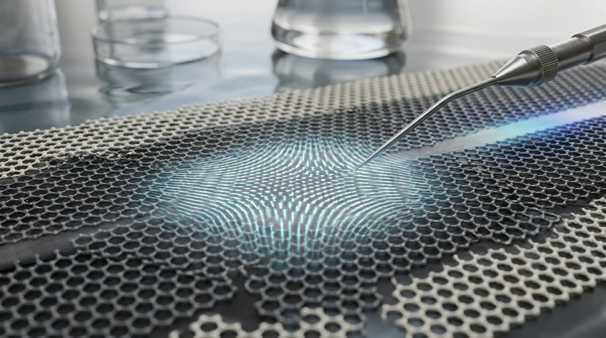
To understand how this works, imagine taking two identical mesh screens and laying one directly over the other. If they are perfectly aligned, you just see a single, dense mesh. But if you rotate one screen by just a few degrees, a new, much larger pattern appears where the wires overlap. This new, larger pattern is called a moiré pattern.
In the world of nanotechnology, researchers are doing something similar with atoms. By taking a single layer of carbon (graphene) and stacking it on top of a layer of hexagonal boron nitride (hBN) at a very specific, slightly misaligned angle, they create a moiré superlattice. This superlattice is a new kind of landscape for electrons. Instead of seeing a uniform surface, the electrons see a periodic pattern of hills and valleys created by the interference of the two atomic lattices. This landscape can force electrons into specific arrangements that create the electrical "memory" required for ferroelectricity.
The physics driving this discovery is a complex interplay of symmetry and electronic structure. To achieve ferroelectricity, a material must have broken inversion symmetry. In a perfectly symmetric crystal, the positive and negative charges are balanced in a way that prevents a permanent electric dipole from forming. However, when graphene is stacked with hBN, the different atomic arrangements of the two materials interact.
Graphene consists of a single layer of carbon atoms arranged in a hexagonal lattice. Hexagonal boron nitride, or hBN, is an insulator that shares a similar hexagonal structure but is composed of alternating boron and nitrogen atoms. Because the atomic spacing and the arrangement of these atoms differ slightly, the moiré superlattice acts as a periodic modulation of the electrical potential. This modulation effectively breaks the inversion symmetry of the system.
When this symmetry is broken, the electrons within the graphene layer are no longer distributed uniformly. Instead, they tend to congregate in specific regions of the moiré pattern. This uneven distribution of charge creates an electrical dipole—a separation of positive and negative charges. Because the moiré pattern is periodic and repeats across the entire surface, these dipoles align in a way that creates a macroscopic polarization. The result is a two-dimensional material that behaves like a ferroelectric, capable of holding an electrical state based on its structural arrangement.
In a groundbreaking study, Bao Q. Tu, Tanweer Ahmed, Garen Avedissian, Suzanne Lancaster, Mayank Sharma, Kenji Watanabe, Takashi Taniguchi, Fèlix Casanova, Marco Gobbi, and Luis E. Hueso investigated the electrical properties of these singly aligned graphene-hBN moiré superlattices. Their primary goal was to determine if these structures could exhibit the characteristic signature of ferroelectricity: hysteresis.
Hysteresis is a phenomenon where the output of a system depends on its history. In the context of ferroelectricity, if you apply an electric field to the material, you can force the dipoles to flip and point in a certain direction. When you remove that field, a ferroelectric material does not simply return to its original state; it remains in the new orientation. When you plot the polarization against the applied electric field, you see a loop rather than a straight line. This loop is the "hysteresis loop."
The researchers successfully observed this hysteresis in the graphene-hBN system. They found that the electrical state of the moiré superlattice could be switched and held by an external voltage. This observation is significant because it confirms that the moiré pattern is not just a decorative structural feature, but a functional landscape capable of supporting stable, switchable electrical polarization. This proves that moiré superlattices are a viable platform for studying and utilizing new forms of electronic behavior that do not exist in standard, non-layered materials.
The discovery of ferroelectric hysteresis in these superlattices is a significant milestone in condensed matter physics and materials science. First, it validates the "twistronics" approach—the idea that we can engineer the properties of materials not just by their chemical composition, but by the physical angle at which we stack them. This opens up a virtually infinite playground for material design.
Second, the ability to control polarization through moiré patterns offers a path toward extremely low-power electronics. Since the information is stored in the orientation of the dipoles rather than a continuous flow of current, the energy required to maintain a state is nearly zero. This could revolutionize the design of non-volatile memory, allowing for devices that can remain in a "sleep" mode for years without losing a single bit of data, and wake up instantly when power is applied.
Furthermore, the transition from bulk ferroelectric materials to two-dimensional, atomically thin ferroelectric superlattices allows for unprecedented scaling. As we move toward the limits of silicon, the ability to control electricity at the single-atom layer provides a way to continue shrinking devices without the catastrophic loss of control caused by quantum tunneling and heat.
While these results are highly promising, it is important to distinguish between a fundamental scientific discovery and a commercially viable technology. The research presented by Tu and the team was conducted under highly controlled laboratory conditions, likely involving extremely high-quality, "atomically clean" samples.
One major limitation is the current method of fabrication. Most research at this level utilizes "mechanical exfoliation"—the process of using adhesive tape to peel layers of material off a crystal—to create ultra-thin flakes. This method is excellent for precision but is impossible to scale for mass manufacturing. To make this technology a reality, scientists must develop methods like chemical vapor deposition (CVD) that can grow these moiré superlattices over large, uniform areas of silicon wafers.
Additionally, many of these exotic electronic states are most stable at extremely low temperatures. For these materials to work in a smartphone or a laptop, the ferroelectric effect must be robust and stable at room temperature. While the potential for room-temperature operation is a major area of ongoing research, it has not yet been definitively proven for these specific graphene-hBN moiré systems. Finally, the complexity of controlling the exact twist angle across a large surface remains a significant engineering hurdle.
The implications of this research extend far beyond the laboratory. One of the most exciting potential applications is in neuromorphic computing. This is a branch of computer engineering that seeks to mimic the structure and function of the human brain. Biological neurons communicate through electrical impulses that leave a "trace" or a state in the synapse. The non-volatile, switchable nature of ferroelectric moiré superlattices makes them ideal candidates for creating "artificial synapses" in hardware, allowing computers to learn and adapt much more efficiently than current architectures.
Another application is in the realm of ultra-low-power sensors. Because these materials are incredibly sensitive to external electric fields and mechanical strain, they could be used to create sensors that require almost no power to operate, making them perfect for remote monitoring, environmental sensing, or medical implants.
In the field of data storage, we may see the emergence of a new class of non-volatile memory that bridges the gap between the speed of RAM and the permanence of hard drives. This could lead to "instant-on" computers where the device is always ready, has zero standby power consumption, and is significantly more resistant to the heat-related failures that plague modern high-performance computing.
If you take away only one concept from this research, let it be this: by slightly rotating layers of graphene and hBN, scientists have created a "moiré superlattice" that breaks the symmetry of the atoms, creating a new way to store electrical information through ferroelectric hysteresis.
How do you create a moiré pattern?
A moiré pattern is created when two periodic patterns, such as the lattice of atoms in two different materials, are placed on top of one another with a slight misalignment or rotation. This misalignment causes an interference pattern that creates a new, larger repeating structure.
What is the difference between a conductor and an insulator in this context?
Graphene is a highly conductive material, meaning electrons move through it very easily. hBN is an insulator, meaning it resists the flow of electricity. When they are stacked, the hBN acts as a template that shapes the way electrons behave in the graphene, allowing for the creation of the moiré pattern.
Why is "hysteresis" important for memory?
Hysteresis means the material's state depends on its history. In memory applications, this means that if you apply a voltage to flip an electrical state, the material will stay in that state even after you turn the voltage off. This is the definition of non-volatile memory.
What is the significance of "broken inversion symmetry"?
In many crystals, the arrangement of atoms is perfectly symmetric, meaning the top and bottom (or left and right) look identical. This symmetry prevents a permanent electrical charge imbalance. By using a moiré pattern to break this symmetry, we can create a permanent electrical imbalance, which is required for ferroelectricity.
Can this technology replace silicon today?
No, it is not ready for mass production. While the science is proven in a lab setting, the manufacturing processes required to produce these atomically perfect, twisted layers at scale do not yet exist. It is a long-term, fundamental technology rather than a short-term replacement.
The work by Bao Q. Tu, Tanweer Ahmed, and their colleagues represents a profound step forward in our ability to control matter at its most fundamental level. By moving beyond the chemical composition of materials and into the realm of structural geometry through moiré superlattices, we are uncovering entirely new ways to manipulate electricity. While challenges in scalability and temperature stability remain, the discovery of ferroelectric hysteresis in these systems provides a clear roadmap toward a future of more efficient, more powerful, and more intelligent electronics. The ability to "program" the very structure of an atomic lattice may be the key to unlocking the next era of human computing.
Serious about B2B integration? Test our premium Pulsed Electrical Resistive Carbon Heating turbostratic graphene in your lab. 100g sample packs available now.
Explore More
Researchers discover naturally formed graphene sheets and carbon ovals in stingless bee hives, creating a novel emergent material with powerful blue light...

Discover how rippled graphene pores act as fluidic memristors, enabling advanced synaptic functionalities for the next generation of neuromorphic computing.

Learn how to use electromechanical responses in gapped graphene to measure electronic temperature and band gaps using traveling flexural waves.