
Nature's Nanotech: Graphene and Blue Emission Found in Bee Hives
Researchers discover naturally formed graphene sheets and carbon ovals in stingless bee hives, creating a novel emergent material with powerful blue light...
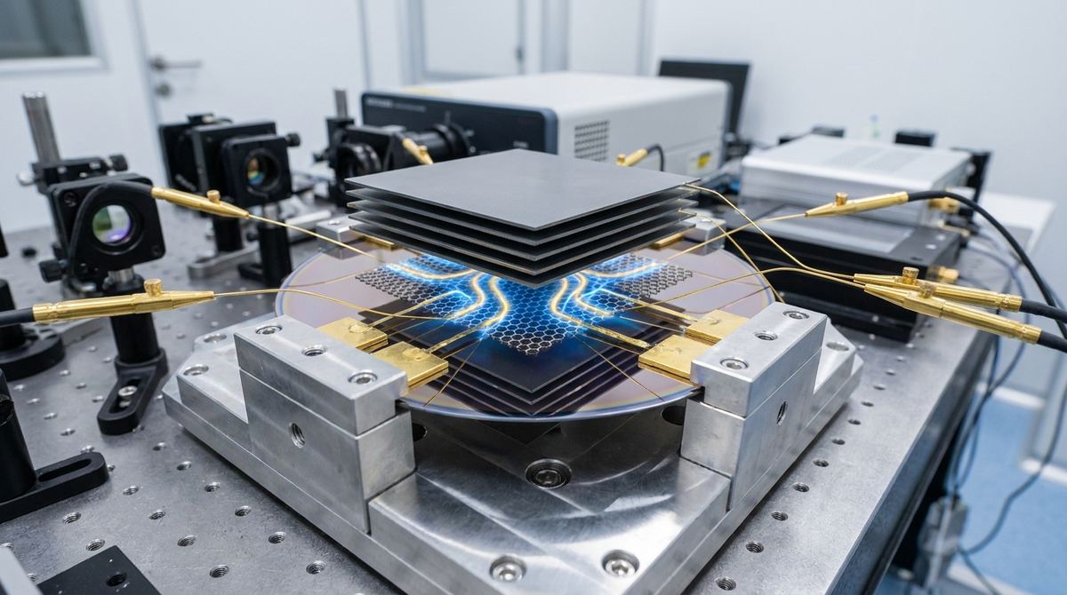
In the development of next-generation quantum materials, one of the most persistent challenges is the inability to distinguish between the effects of disorder and the effects of electron-electron interactions. When a two-dimensional material undergoes a phase transition, such as a quantum Hall plateau transition, the observed behavior is often a convolution of both factors. For engineers working on quantum sensors, topological electronics, or moiré-based devices, this ambiguity makes it difficult to predict how a device will perform when scaled or when environmental noise is introduced.
Recent research has demonstrated a method to break this deadlock. By using a dual-gated graphene architecture, it is possible to geometrically tune the range of Coulomb interactions. This is achieved by adjusting the distance between the graphene layer and a graphite gate. This technique allows an engineer to selectively modify the dynamical sector of a phase transition (the dynamical exponent, z) while leaving the localization-length exponent (gamma) unchanged. This guide provides a blueprint for building a prototype device capable of this level of interaction control.
The goal is to construct a graphene heterostructure that allows for the independent tuning of electronic screening. By varying the thickness of a hexagonal Boron Nitride (hBN) dielectric layer between the graphene and a graphite gate, you can transition the system from an unscreened regime (where interactions are long-range) to a screened regime (where interactions are short-range).
The success of the prototype is measured by the ability to observe a shift in the dynamical exponent z from approximately 1 to 2, while the localization-length exponent gamma remains constant at approximately 2.4. This capability transforms a static material into a tunable platform for studying correlated electronic phases.
To achieve the precision required for these measurements, the following materials and equipment are necessary:
1. Graphene: High-mobility, single-layer graphene. For laboratory-scale prototyping, exfoliated graphene is preferred over CVD graphene due to the lower density of grain boundaries and defects.
2. Hexagonal Boron Nitride (hBN): This serves as the dielectric layer. You will need multiple flakes of varying thicknesses. For this application, thicknesses should range from 10 nm to 100 nm.
3. Graphite Gates: Highly doped graphite flakes. Graphite is used instead of metal gates because it provides a smoother electrostatic potential, which is critical for maintaining high carrier mobility in the graphene.
4. Substrate: A silicon wafer with a thick thermal oxide layer (typically 285 nm to 300 nm) to act as a global back-gate.
5. Contacts: Gold and Titanium for electrical interconnects.
6. Equipment:
- An electron-beam lithography (EBL) system for fine-patterning.
- A dry-transfer setup (polymeric handles like PC or PDMS) for stacking the heterostructure.
- A high-field superconducting magnet (minimum 10 Tesla, though 14T+ is ideal).
- A dilution refrigerator capable of reaching temperatures below 100 mK.
The fabrication of a dual-gated device requires a precise stacking sequence, typically performed via a dry-transfer method to prevent contamination.
1. Substrate Preparation: Clean the silicon/SiO2 substrate using oxygen plasma or specialized cleaning solvents to ensure no organic residue remains.
2. Bottom Gate Depstrate: Pick up a flake of highly doped graphite using a polymer handle. Transfer it onto the substrate. This graphite flake will act as your primary tuning gate.
3. Dielectric Layer Depstrate: Pick up a flake of hBN. The thickness of this flake is your most critical variable. To test the transition from unscreened to screened regimes, you should prepare several devices with hBN thicknesses of 10 nm, 30 nm, 60 nm, and 100 nm.
4. Graphene Placement: Pick up a single layer of high-quality graphene and place it directly on top of the hBN layer.
5. Encapsulation: Pick up a second, thicker flake of hBN (approximately 20-30 nm) and place it over the graphene. This encapsulates the active region, protecting it from environmental degradation and reducing charge noise.
6. Contact Patterning: Use electron-beam lithography to define the contact areas. Deposit Titanium/Gold through a suspended resist mask to create the electrical leads.
7. Final Cleaning: Perform a gentle thermal anneal in a vacuum or a forming gas (H2/Ar) environment to remove any residual polymer from the contact areas.
Once the device is fabricated, the validation requires a two-pronged scaling analysis under high magnetic fields and cryogenic temperatures.
1. Setup: Place the device in a dilution refrigerator equipped with a superconducting magnet. Apply a perpendicular magnetic field to enter the quantum Hall regime.
2. Temperature Scaling: Measure the longitudinal resistance (Rxx) as a function of temperature (T) at the transition point between two quantum Hall plateaus. The resistance should follow a scaling law where the width of the transition scales with T raised to the power of kappa (k).
- Note: Kappa is defined as 1/(z gamma).
3. Current Scaling: Perform a second set of measurements by varying the source-drain current (I) at a constant temperature. The resistance scaling with current provides an independent way to extract the dynamical exponent z.
4. Data Analysis:
- Calculate kappa from the temperature scaling.
- Use the current scaling results to solve for z.
- Once z is known, calculate gamma using the relationship gamma = 1 / (kappa z).
5. Success Metric: If the device is working correctly, as you increase the hBN thickness (increasing screening), you should observe z shifting from ~1 to ~2, while gamma remains stable at ~2.4.
The following assumptions are made for this prototype design:
- Dielectric Thickness: We assume that hBN thicknesses between 10 nm and 100 nm are sufficient to transition between the screened and unscreened regimes.
- Thermal Stability: We assume the system can reach a base temperature of at least 100 mK to resolve the scaling behavior.
- Magnetic Field: We assume a magnetic field of at least 10T is available to reach the quantum Hall regime for the specific graphene sample.
Safety Note: When working with high-field superconducting magnets, ensure all non-magnetic tools are used and follow all laboratory protocols regarding quench protection and magnetic field exposure.
1. Dielectric Breakdown: The hBN layer is very thin. High voltages applied to the graphite gate could cause electrical breakdown.
- Mitigation: Use a slow voltage ramp and monitor the leakage current continuously during the initial testing phase.
2. Contamination: Even a single layer of water or polymer residue can ruin the mobility of the graphene.
- Mitigation: Perform all transfers in a controlled environment (like a glovebox) and use high-vacuum annealing steps.
3. Contact Resistance: High contact resistance can mask the scaling behavior of the graphene.
- Mitigation: Use a multi-step lithography process and ensure the Ti/Au contacts are deposited with high adhesion and low resistivity.
4. Thermal Decoupling: At mK temperatures, the electron temperature may be higher than the thermometer reading.
- Mitigation: Use low excitation currents during measurements to prevent electron heating.
This guide is based on the research findings of Chanda et al. (2026), "Screening-controlled dynamical criticality in the quantum Hall regime." The specific values for the exponents (z ~ 1 to 2, and gamma ~ 2.4) and the methodology of using dual-graphite-gated devices to separate dynamical and localization-length exponents are derived directly from the experimental results presented in the source.
Serious about B2B integration? Test our premium Pulsed Electrical Resistive Carbon Heating turbostratic graphene in your lab. 100g sample packs available now.
Explore More
Researchers discover naturally formed graphene sheets and carbon ovals in stingless bee hives, creating a novel emergent material with powerful blue light...

Discover how rippled graphene pores act as fluidic memristors, enabling advanced synaptic functionalities for the next generation of neuromorphic computing.

Learn how to use electromechanical responses in gapped graphene to measure electronic temperature and band gaps using traveling flexural waves.