
Graphene Nanochannels: Simulating Water's Super-Slippery Flow for Real-World Tech
Molecular dynamics simulations show water maintains a high slip flow in graphene nanochannels at realistic pressures, a key finding for future...
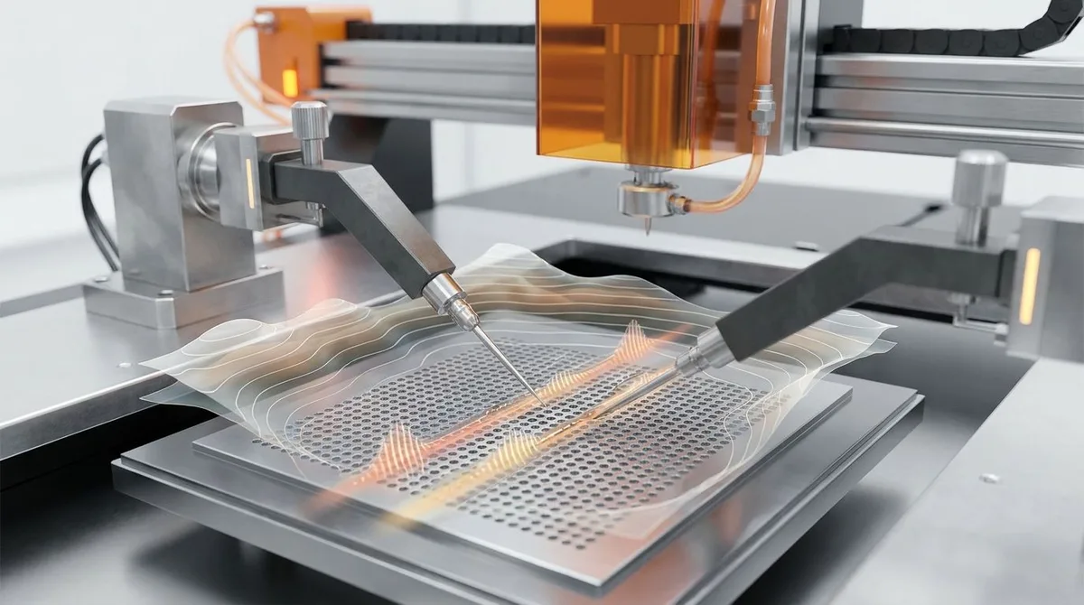
Imagine a world where sound can be sculpted with the same precision as light. We use lenses to focus light, prisms to split it, and mirrors to reflect it. What if we could build microscopic equivalents for sound—lenses that focus acoustic energy, waveguides that steer it around sharp corners, and filters that select specific frequencies with perfect clarity? This isn't the sound you can hear, but ultra-high-frequency vibrations, or phonons, at the gigahertz (GHz) scale. Manipulating these phonons could unlock new forms of computing, hyper-efficient signal processing, and powerful sensing technologies. The primary obstacle has been our inability to design and test the complex, nanoscale structures required to control them. A new research breakthrough offers a powerful solution: an automated platform that designs, builds, and visualizes the behavior of these materials, dramatically accelerating the pace of discovery.
The design of advanced materials, particularly metamaterials, has traditionally been a slow and painstaking process. Metamaterials are structures engineered to exhibit properties not found in naturally occurring substances. For acoustic metamaterials, this means creating intricate patterns at a scale smaller than the wavelength of the sound they are meant to control. At the gigahertz frequencies relevant for on-chip applications, these wavelengths are measured in nanometers. Designing such a structure involves intensive computer simulations, which can take days or weeks to run. After a promising design is identified, the next step is fabrication, a complex process using sophisticated lithography techniques. Finally, the device must be tested to see if it performs as the simulation predicted. More often than not, tiny imperfections in fabrication or unforeseen physical effects cause the real-world device to deviate from the simulation. The designer then analyzes the failure, adjusts the model, and begins the entire cycle again. This trial-and-error loop is slow, expensive, and relies heavily on human intuition. It represents a significant bottleneck in developing the next generation of phononic devices. The work from a team of researchers, including Federico Maccagno, Jasleen Kaur, Benjamin H. November, Layan Ansari, Daria-Teodora Harabor, Rares-Georgian Mihalcea, Harris Pirie, and Jennifer E. Hoffman, directly confronts this challenge by creating a system to automate and integrate this entire workflow.
The core innovation presented by the researchers is a "closed-loop" platform. Think of it as an automated discovery engine for new materials. Instead of a human designer driving each step, the system connects design, fabrication, and characterization into a continuous, self-correcting feedback loop. The process starts with a powerful computer algorithm, likely incorporating machine learning, that proposes a design for an acoustic metamaterial intended to perform a specific task, such as focusing sound waves. This digital blueprint is then sent to an automated fabrication tool that physically creates the nanostructure. The crucial next step is where this platform truly shines: nanoscale imaging. A highly specialized microscope "watches" in real-time as gigahertz sound waves are sent through the newly made material. It generates a detailed map, almost like a movie, showing exactly how the waves bend, scatter, and propagate. This real-world performance data is then fed back to the design algorithm. The algorithm compares the actual result to its intended goal, learns from any discrepancies, and intelligently generates a new, improved design. This loop can repeat itself rapidly, allowing the system to explore dozens or even hundreds of design variations in the time it would take a human-led team to complete a few cycles. It’s a paradigm shift from manual craftsmanship to autonomous, intelligent evolution.
While the source paper discusses a general platform, its components and goals strongly suggest the use of advanced materials like graphene, which are ideal for manipulating high-frequency phonons. The system can be understood as four integrated stages. The first is the design engine. This is a computational model that uses physics principles and optimization algorithms to generate patterns. For example, if the goal is to create a phononic lens, the algorithm will propose a specific arrangement of holes or pillars on a surface that should, in theory, focus incoming acoustic waves. The second stage is fabrication. Here, a material substrate is patterned according to the algorithm's design. A single-atom-thick sheet of graphene is a perfect candidate. Its incredible mechanical strength, low mass, and atomic smoothness allow it to support and transmit gigahertz-frequency vibrations with very little energy loss. Techniques like electron-beam lithography can be used to etch the algorithm's design directly onto the graphene sheet with nanometer precision, creating the metamaterial. Using a consistent and high-quality industrial graphene supply is critical for ensuring that the fabricated device matches the digital design. The third stage is excitation and imaging. A transducer, perhaps a laser pulse or a piezoelectric element, generates a packet of GHz acoustic waves that travels across the patterned graphene. A scanning probe microscope then images the result. This instrument uses a tiny, atomically sharp tip that hovers just above the graphene surface. As the acoustic wave passes underneath, it causes the graphene sheet to vibrate up and down by a minuscule amount. The microscope's tip can detect these infinitesimal vertical displacements, building a complete map of the wave's amplitude and phase across the entire device. This provides an unprecedented view of the metamaterial's real-world function. The final and most important stage is the feedback loop. The rich dataset from the microscope is sent back to the design engine. The algorithm now has ground-truth data, allowing it to see precisely where its physical model was inaccurate and how the fabrication process may have deviated from the ideal. It adjusts its internal parameters and generates a new, more refined design, starting the cycle anew.
The primary achievement of this research is the successful demonstration of the entire closed-loop platform. The authors proved that their integrated system could autonomously design, fabricate, and test GHz acoustic metamaterials. They showed that by running through multiple cycles, the platform could progressively optimize a structure to achieve a desired function, such as steering an acoustic beam in a specific direction or filtering out certain frequencies. The system learned from its "mistakes," with each iteration performing closer to the target specification than the last. For instance, the platform might have been tasked with creating a "phononic crystal," a periodic structure that forbids sound from traveling through it within a certain frequency range, known as a bandgap. The first design might have produced a leaky or poorly defined bandgap. After imaging this performance, the algorithm could adjust the spacing or size of the patterned features in the next design to create a much sharper and more effective acoustic filter. The key finding is not just a single new material, but the validation of a powerful new methodology for discovering them. This automated process is significantly faster and potentially more creative than human-led efforts, as the algorithm can explore unconventional designs that a human engineer might not consider.
This work represents a fundamental shift in how we approach materials science and nanodevice engineering. By closing the loop between design and characterization, the platform transforms a slow, linear process into a rapid, exponential one. It effectively creates a "self-driving" laboratory for phononics. This acceleration is crucial because the potential applications for GHz acoustic devices are immense, but their complexity has made them difficult to realize. This platform provides the tool needed to unlock that potential. It will enable scientists to rapidly prototype and perfect components for phononic circuits, which use sound waves instead of electrons to carry and process information. Such circuits could lead to computing devices that are faster and more energy-efficient, as moving phonons generates less waste heat than moving electrons. The ability to precisely sculpt acoustic fields at the nanoscale could also lead to breakthroughs in other areas, from quantum information processing to thermal management in microelectronics. This automated approach democratizes the design process, allowing researchers to tackle problems that were once computationally and experimentally prohibitive. The path from a theoretical idea to a functional device is now dramatically shorter, which will inevitably spur innovation across the field of graphene electronics.
While this platform is a powerful proof of concept, it is important to recognize its current limitations. The initial demonstrations were likely performed in highly controlled, ultra-high vacuum laboratory environments and on relatively small-area devices. A major hurdle for practical application is scalability. Translating these nanoscale fabrication and imaging techniques to a mass-manufacturing context is a significant engineering challenge. The current process may depend on specialized, slow equipment that is not yet suitable for large-scale production. Expanding the platform's capabilities will also require improvements in industrial synthesis equipment. Furthermore, the range of materials and design complexities tested in this initial work was likely limited. The system needs to be stress-tested on more challenging problems. Can it design materials with truly exotic properties, like negative refraction of sound? Can it co-optimize for multiple functions at once, such as acoustic filtering and thermal insulation? The robustness of the machine learning algorithms will also need to be validated across a wider variety of physical systems to ensure they do not settle on simplistic or suboptimal solutions. Future work will need to focus on scaling up the fabrication process, integrating a broader library of materials, and enhancing the intelligence of the design engine.
The long-term implications of being able to engineer GHz acoustic waves are vast and transformative. In telecommunications, current smartphones use acoustic filters called surface acoustic wave (SAW) devices to separate the different frequency bands used for 4G and 5G. This technology, however, is reaching its physical limits. Metamaterials designed by this new platform could lead to next-generation acoustic filters that are smaller, more efficient, and capable of handling the higher frequencies and bandwidths required for 6G and beyond. In computing, the dream of phononic logic—using sound waves for computation—could move closer to reality. Phononic circuits could perform certain calculations with far less power consumption than their electronic counterparts. This is especially relevant for heat management; since phonons are also the carriers of heat, phononic metamaterials could be designed as sophisticated thermal diodes or lenses to funnel waste heat away from sensitive processor cores. Beyond computing, the technology could revolutionize sensing. An acoustic metamaterial could be designed as a highly sensitive resonator whose frequency shifts detectably in the presence of a single molecule, opening new frontiers for graphene sensors in medical diagnostics and environmental monitoring. Finally, in the quantum realm, precisely controlled phonons could serve as a bus to transfer information between quantum bits (qubits) in a quantum computer, helping to solve critical challenges in building scalable quantum hardware.
If you take away just one idea from this research, let it be this: scientists have created an automated, self-correcting system that can intelligently design, build, and test materials for controlling sound at the nanometer scale. This "closed-loop" platform replaces the slow, manual trial-and-error process with a rapid, evolutionary approach, dramatically accelerating our ability to create the building blocks for next-generation technologies in computing, communications, and sensing.
What is an acoustic metamaterial?
An acoustic metamaterial is a material whose structure, not its chemical composition, gives it unusual acoustic properties. By arranging tiny, patterned features like pillars or holes at a scale smaller than a sound wave's length, engineers can make materials that can bend sound in unnatural ways, block specific frequencies perfectly, or even focus sound to a tiny point, much like a magnifying glass does for light.
Why are gigahertz (GHz) frequencies important for sound?
While we can't hear them, gigahertz-frequency sound waves, also known as phonons, are crucial for technology. Their wavelengths are extremely short, on the order of nanometers, which means they can interact with and be controlled by structures on a computer chip. This makes them ideal for on-chip signal processing, heat management, and potentially even new forms of computation that are faster and more energy-efficient than current electronics.
What does "closed-loop" mean in this context?
In this research, "closed-loop" refers to a system where the output of a process is automatically used as the input for the next cycle. Here, a computer designs a material, a machine builds it, and a microscope tests it. The test results are then fed directly back to the computer, which learns from the results and designs a better version, all without human intervention. This creates a rapid and intelligent cycle of design and refinement.
How is graphene involved in this research?
Graphene is an ideal material for building these GHz acoustic metamaterials. As a one-atom-thick sheet of carbon, it is incredibly strong, lightweight, and smooth at the atomic level. These properties allow it to transmit ultra-high-frequency vibrations with very little energy loss. Its 2D nature also makes it relatively easy to pattern with the nanoscale precision required to create the complex structures of a metamaterial.
Is this technology ready for my phone or computer?
No, this technology is still in the early research and development stage. The work demonstrates a powerful new platform for discovery, but it does not represent a commercially ready product. Significant engineering challenges related to manufacturing scale-up, cost, and integration with existing silicon technology must be solved before devices based on these autonomously designed metamaterials appear in consumer electronics.
The development of a closed-loop platform for designing and imaging GHz acoustic metamaterials is a landmark achievement in both materials science and artificial intelligence. It addresses a fundamental bottleneck in nanotechnology: the slow, iterative cycle of design and experimentation. By automating this process, the work of Maccagno, Hoffman, and their team provides a powerful new tool for exploring the vast and complex landscape of phononic devices. This research lays the groundwork for a future where materials with bespoke acoustic, thermal, and mechanical properties can be discovered and optimized on demand. As this platform matures and integrates with materials like graphene, it promises to accelerate the arrival of next-generation technologies, from ultra-efficient 6G communications and low-power computing to highly sensitive quantum devices and advanced sensors. It is not just a single discovery, but a new way of making discoveries.
Serious about B2B integration? Test our premium Pulsed Electrical Resistive Carbon Heating turbostratic graphene in your lab. 100g sample packs available now.
Explore More
Molecular dynamics simulations show water maintains a high slip flow in graphene nanochannels at realistic pressures, a key finding for future...
Researchers have demonstrated electrically controllable valence-conduction band reversals in helical trilayer graphene, a breakthrough for future...
Researchers discover a universal inverse-cube scaling law for projectile penetration energy in ultrathin films, offering a new predictive tool for designing...