A Universal Law for Projectile Penetration Energy in Ultrathin Films
Researchers discover a universal inverse-cube scaling law for projectile penetration energy in ultrathin films, offering a new predictive tool for designing...
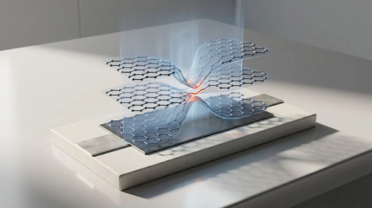
Imagine a material that can be instantly rewired at the most fundamental level. Not just switched from on to off, but transformed from one type of electronic material into another with the flip of a switch. This is the frontier of materials science, a realm where we can program the very identity of matter. A recent breakthrough in the study of graphene has brought this science fiction concept a step closer to reality. By precisely stacking three layers of graphene into a unique helical structure, researchers have shown that they can use a simple electric field to force the material's fundamental electronic bands to swap places, a feat with profound implications for the future of computing.
Modern electronics are built on the silicon transistor, a tiny switch that controls the flow of electrons. For decades, progress has been defined by making these transistors smaller and faster. However, we are now approaching the fundamental physical limits of silicon. As components shrink to the scale of mere atoms, quantum effects and heat generation become insurmountable problems. To continue the advance of computing power, scientists are searching for new materials and new principles of operation. The goal is to find a successor to the simple on-off switch—a device whose properties can be more dynamically and efficiently controlled. This is the challenge addressed by a team of researchers including Matan Bocarsly, Indranil Roy, Weifeng Zhi, Li-Qiao Xia, Aviram Uri, Yves H. Kwan, Aaron Sharpe, Matan Uzan, Yuri Myasoedov, Kenji Watanabe, Takashi Taniguchi, Trithep Devakul, and their colleagues. They sought to create a system where a fundamental electronic property, not just current flow, could be actively tuned by an external voltage.
To understand the breakthrough, we can think of the electrons in a material as living in a multi-story building. The "valence band" is like the ground floor, where electrons are comfortably settled and don't contribute to electrical current. The "conduction band" is like an upper floor, where electrons can move freely, creating a current. In an insulator or semiconductor, there's an energy gap—a staircase—between these floors. An electron needs a jolt of energy to climb the stairs and start conducting. The core idea of this research is that in a special material, helical trilayer graphene, it's possible to use an electric field to make the ground floor and the upper floor swap places. This "band reversal" or "band inversion" fundamentally changes the rules for how electrons can move. The material's electronic identity is transformed. The key is the unique structure: three layers of graphene stacked with a slight twist, creating a helical arrangement that makes this electrical control possible.
The system's magic lies in its precise architecture. It starts with graphene, a single layer of carbon atoms arranged in a honeycomb lattice. While a single layer has remarkable properties, stacking multiple layers introduces new and complex physics. The way the layers are stacked is critically important. In this work, the researchers constructed a "helical trilayer," which implies a specific, non-standard stacking order that twists as you move from one layer to the next. This controlled twist creates a larger-scale interference pattern known as a moiré superlattice. This superlattice acts as a new, artificial landscape for the electrons, profoundly altering their energy levels and behavior. This precision-engineered structure is the opposite of randomly stacked graphene, such as the material found in bulk graphene powder, where the layers are misaligned without long-range order.
The device itself is fabricated much like a standard field-effect transistor. The helical trilayer graphene is placed on an insulating substrate, with a metallic gate electrode underneath. By applying a voltage to this gate, a vertical electric field is generated that passes through the graphene layers. This electric field acts as a tuning knob. It creates a potential difference between the top and bottom layers of the trilayer stack, effectively "pulling" on the electron energy levels. In most materials, this would only slightly shift the energy bands. However, due to the unique electronic structure created by the helical moiré pattern, this electric field can push the energy of the valence band up and the conduction band down until they cross over and invert their positions. This is the electrically controllable band reversal.
The research team successfully demonstrated and measured this band inversion. Using advanced electrical transport measurement techniques, likely performed at cryogenic temperatures to minimize thermal noise, they charted the material's electronic behavior as they varied the gate voltage. They observed a dramatic change in the material's conductivity that corresponded precisely with the theoretical predictions for a band inversion. At a specific value of the electric field, the energy gap between the valence and conduction bands closes, and then re-opens with the bands swapped. This transition point represents a topological phase transition, where the fundamental electronic character of the material is altered. The research categories of "Mesoscopic and Hall Effect" and "Strongly Correlated Electrons" suggest that they likely used magnetic fields to probe the nature of these electronic states and may have observed exotic phenomena near the inversion point where interactions between electrons become dominant, leading to collective behaviors not seen in ordinary materials. They effectively proved that the electronic ground floor and first floor of their material could be swapped on demand using a voltage.
This discovery is significant because it represents a new paradigm for an electronic switch. A conventional transistor controls the quantity of charge carriers, switching between a high-conductivity "on" state and a low-conductivity "off" state. This new system controls the qualitative nature of the charge carriers themselves. It switches the material between different fundamental electronic phases. This capability is a cornerstone of the emerging field of topological electronics. Topological electronic states are exceptionally robust; because their properties are locked in by the overall structure of the energy bands, they are less susceptible to being disrupted by local defects or impurities in the material. A device that can switch between a conventional state and a topological state could store information in the phase itself, leading to more stable and energy-efficient forms of memory and logic. It moves beyond simply controlling current and toward controlling the quantum mechanical fabric of the material itself.
While groundbreaking, this research is a proof of concept performed under highly controlled laboratory conditions. The primary limitation is temperature. These delicate quantum phenomena are typically only observable at extremely low temperatures, close to absolute zero. A major challenge will be to see if similar effects can be engineered into a material that operates at room temperature. Another significant hurdle is fabrication. Creating helical trilayer graphene with the precise twist angle required is an incredibly difficult process that is not yet scalable. The long-term stability and reliability of these devices also need extensive testing. Scientists will need to investigate how fast this band inversion can be switched, how many times it can be cycled before the material degrades, and how sensitive the effect is to imperfections. The path from this fundamental discovery to a commercial product involves overcoming substantial engineering and manufacturing challenges, a common theme in the world of advanced graphene manufacturing techniques.
Although direct commercial applications are years or even decades away, the potential is enormous. This electrically controllable band structure could form the basis of a new class of ultra-low-power logic devices called topological transistors. Instead of stopping current, they would switch the topological state of a channel, which could theoretically require much less energy. The ability to switch between distinct electronic phases could also be used to create reconfigurable circuits, where the function of a component could be changed in real-time by a control voltage. Furthermore, this system provides an exciting new platform for fundamental physics research, particularly in the quest for topological quantum computing. The protected electronic states at the boundaries between different topological domains could potentially host robust quantum bits, or qubits, the building blocks of quantum computers. This research fits squarely into the future landscape of graphene electronics, pushing the boundaries of what is possible with carbon-based materials.
The most important takeaway is that by stacking three layers of graphene in a specific twisted, helical arrangement, scientists can use a simple electric voltage to fundamentally rewire the material's electronic identity, swapping the energy bands that define whether it acts as one type of material or another.
What are valence and conduction bands?
In simple terms, think of the valence band as the default energy state where electrons reside in a material, keeping them bound to their atoms. The conduction band is a higher energy state where electrons can move freely and conduct electricity. The separation between them, the band gap, determines if a material is an insulator, semiconductor, or metal.
What is trilayer graphene?
Trilayer graphene is a material made of three individual, one-atom-thick sheets of graphene stacked on top of one another. The electronic properties of the trilayer system are highly dependent on the precise alignment and stacking order of these three layers, giving rise to much richer physics than a single sheet alone.
Why is the helical structure important?
The "helical" or twisted structure is the key innovation. This specific stacking arrangement creates a moiré superlattice, a larger repeating pattern that modifies the electronic environment. This new, engineered landscape is what makes the electron energy bands so sensitive to an external electric field, enabling the dramatic band reversal that the researchers observed.
What does electrically controllable mean for electronics?
"Electrically controllable" is the foundation of all modern electronics. It means you can use a voltage to change a property of a material. In a standard transistor, you control the flow of current. In this advanced research, a voltage is used to control a much more fundamental property: the very structure of the material's electronic bands.
Is this technology ready for my phone?
No, not anytime soon. This is fundamental, exploratory research conducted in a laboratory at very low temperatures. It demonstrates a new physical principle. While it opens exciting possibilities for future generations of electronics, the challenges of room-temperature operation and scalable manufacturing mean it is still many years away from being integrated into consumer devices.
The demonstration of electrically controllable band reversals in helical trilayer graphene is a landmark achievement in condensed matter physics and materials science. It showcases an unprecedented level of control over the quantum mechanical properties of a material. By moving beyond simply gating conductivity and toward actively reconfiguring a material's electronic topology, this work opens a new design space for post-silicon electronics. While the practical hurdles of temperature and manufacturing remain significant, this research provides both a vital tool for exploring exotic quantum phenomena and a tantalizing glimpse into a future of programmable, topological, and profoundly more efficient electronic systems.
This research points toward a practical lesson: graphene-based materials are most powerful when their nanoscale properties are connected to a clear engineering problem. The result is not a finished commercial product by itself, but it gives researchers and manufacturers a better map for designing lighter, more sensitive, or more durable systems. Future work still needs testing under real operating conditions, but the direction is promising because it joins materials science with application-driven design.
Serious about B2B integration? Test our premium Pulsed Electrical Resistive Carbon Heating turbostratic graphene in your lab. 100g sample packs available now.
Explore More
Researchers discover a universal inverse-cube scaling law for projectile penetration energy in ultrathin films, offering a new predictive tool for designing...

Explore how researchers use machine learning to design a high-capacity Janus aminobenzene-graphene anode, a breakthrough for next-generation sodium-ion...
Discover how carbon nitride monolayer nanosheets, a graphene analogue, are providing critical insights into how stars form by solving the cosmic puzzle of...