
3D Atomic Imaging of Graphene Dynamics from a Single Low-Dose TEM Snapshot
A new physics-informed AI method reconstructs the 3D atomic structure and dynamics of graphene from a single low-dose TEM image, solving a key imaging...
The digital world is built on bits—the ones and zeros that encode information. For decades, we have stored these bits by controlling the flow of electric charge in transistors or by flipping the magnetic state of tiny ferromagnetic domains on a hard drive. But as our demand for faster, smaller, and more energy-efficient devices grows, these conventional methods are approaching their physical limits. A new paradigm, called spintronics, aims to use another property of the electron: its intrinsic spin, a quantum mechanical version of a tiny spinning top with a north and south pole. The challenge has been finding the right materials to manipulate and read this spin efficiently. Now, a groundbreaking study provides a new path forward, demonstrating the ability to see the state of a promising new type of magnetic material at the ultimate atomic limit.
The field of spintronics has long been interested in a class of materials known as antiferromagnets (AFMs). Unlike the ferromagnets in a typical refrigerator magnet, where all electron spins align in the same direction to create a strong external magnetic field, the spins in an antiferromagnet are arranged in a perfectly alternating, up-down-up-down pattern. This opposing arrangement means their net external magnetic field is zero. This property makes them incredibly attractive for data storage; they are immune to erasure by external magnetic fields and, because they don’t interact with their neighbors, they can be packed together at extreme densities. They also have the potential to be switched thousands of times faster than ferromagnets. The problem is that the very property that makes them so appealing—their lack of an external magnetic field—also makes them extraordinarily difficult to read and write. How do you detect a magnetic state if it produces no magnetic signal? This is the central challenge that has hindered the development of AFM-based spintronics. Research by Affan Safeer, Calisa Dias, Mahdi Ghorbani-Asl, Abdallah Karaka, Pradyumna Bawankule, Weibin Li, Pierluigi Gargiani, Wouter Jolie, Arkady V. Krasheninnikov, Amilcar Bedoya-Pinto, Thomas Michely, and Jeison Fischer directly confronts this problem by developing a method to visualize the magnetic state of a single-layer AFM, chromium sulfide (Cr2S3), with atomic precision.
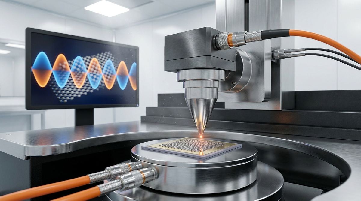
To solve the problem of "seeing" the invisible magnetic order, the research team used a technique called spin-polarized scanning tunneling microscopy (SP-STM). Imagine trying to read Braille not with your finger, but with a tiny magnetic needle. An SP-STM works on a similar principle. It uses an atomically sharp metallic tip, which is itself magnetic, and brings it incredibly close to the surface of the material being studied—in this case, a single atomic layer of Cr2S3. A small voltage is applied, causing electrons to "tunnel" across the tiny gap between the tip and the surface, creating a measurable electric current. The key is that the amount of current that flows depends on the relative alignment of the magnetic spin on the tip and the magnetic spin of the atom directly below it. If the spins are aligned (e.g., both "up"), more current flows. If they are anti-aligned (one "up," one "down"), less current flows. By scanning this magnetic tip across the entire surface and recording the tunneling current at every point, the researchers could construct a complete, atom-by-atom map of the material's hidden magnetic landscape. This allowed them not only to confirm the alternating up-down spin structure but, most importantly, to watch it change in real time.
The active material at the heart of this experiment is a two-dimensional layer of chromium sulfide, Cr2S3. In this material, the chromium atoms act as tiny magnets, each with its own electron spin. The sulfur atoms help to mediate the interactions between them, forcing them to adopt the energetically favorable antiferromagnetic order. Creating and studying a pristine, single atomic layer of such a material is an immense technical challenge, often requiring an atomically flat and unreactive substrate for support. While the paper focuses on the Cr2S3 itself, in the context of building a functional device, this 2D magnet would need to be integrated with other components. This is where materials like graphene become essential. Graphene, with its exceptional electrical conductivity and atomic thinness, could serve as the perfect electrode. In a future memory cell, a graphene layer could be used to apply a precise electric field or pass a spin-polarized current to controllably "write" the magnetic state of the Cr2S3, while another layer could help in the readout process. The system studied by the researchers, therefore, represents the core magnetic component of what could become a complex heterostructure, where different 2D materials are stacked like pages in a book to create novel graphene electronics. The SP-STM instrument itself acts as the external probe, the "reader" that reveals the fundamental physics at play. Its operation relies on the principles of quantum mechanics, specifically the spin-dependent tunneling that translates the magnetic property of spin into a measurable electrical signal.
The primary achievement of the study was the direct, real-space visualization of the antiferromagnetic order in monolayer Cr2S3. The images produced by the SP-STM clearly showed the expected checkerboard-like pattern of alternating magnetic contrast, a direct signature of the opposing spin orientations on neighboring chromium atoms. This was a critical validation of the material's intrinsic magnetic properties at the 2D limit. The most significant finding, however, was the observation of "Néel vector switching." The Néel vector is a concept used to describe the overall orientation of the alternating spin axis. For example, the up-down pattern might be aligned along the material's horizontal axis. The researchers found that this entire ordered pattern could spontaneously or be induced to reorient, for instance, to align along the vertical axis. By taking a series of images over time, they captured snapshots of the system before and after this switch. This is the first atomic-scale detection of such a dynamic process in this material. It proves that the magnetic state is not frozen in place but represents a degree of freedom that can be changed. In essence, they successfully read two different states of the same material—a "zero" and a "one"—at the atomic scale, providing the foundational evidence needed to consider Cr2S3 for memory applications.
This result is a critical piece of the puzzle for the future of spintronics. By proving that the Néel vector in a 2D antiferromagnet can be detected and that it can switch between different states, the study provides a vital proof-of-concept for AFM-based memory. It moves the idea from theoretical possibility to experimental reality. This opens up a new family of 2D materials for exploration in the field of nanoelectronics and data storage. The ability to read the state is the first of two crucial steps; the next is to develop reliable ways to write it. Understanding the fundamental physics of how and why the Néel vector switches, as revealed by this atomic-scale observation, gives scientists the insights needed to design methods for controlling it, perhaps using electrical fields or spin currents. This could ultimately lead to the development of Antiferromagnetic MRAM (AFM-MRAM) that is significantly denser, faster, and more robust than any memory technology available today. It lays the scientific groundwork for a new generation of computing hardware.
While groundbreaking, this research was conducted under highly controlled laboratory conditions that are far from those of a commercial device. The experiments were performed in an ultra-high vacuum to prevent contamination and at cryogenic temperatures (just a few degrees above absolute zero) to stabilize the magnetic order and minimize thermal noise. A major hurdle for practical applications will be to demonstrate that this antiferromagnetic order and the ability to switch it persist at room temperature. Furthermore, the switching observed in this study was either spontaneous or induced by the localized field of the STM tip. While useful for scientific discovery, this is not a scalable way to write data. The next critical step is to develop and integrate a reliable, low-power writing mechanism, such as applying a voltage pulse through a nearby graphene sensor or electrode structure. The challenges of large-scale, defect-free synthesis of monolayer Cr2S3 also need to be addressed, a common bottleneck for many promising 2D materials that requires advances in graphene production machinery. Finally, the long-term stability of the magnetic states, known as data retention time, must be thoroughly characterized to ensure information can be stored reliably for years.
If the challenges of temperature, writing, and manufacturing can be overcome, the potential applications are transformative. The primary application lies in ultra-high-density data storage. Because AFM bits do not generate stray fields, they can be placed nanometers apart without interfering with each other, promising storage densities that are orders of magnitude beyond current hard drives or solid-state drives. Another key area is ultra-fast computing. The natural resonance frequencies of antiferromagnets are in the terahertz (THz) range, about a thousand times faster than the gigahertz (GHz) clock speeds of modern CPUs. This could enable THz processors and logic circuits, shattering current speed barriers. Furthermore, the inherent stability of the AFM state against external magnetic fields makes it ideal for radiation-hard electronics required in aerospace and defense applications, protecting critical data in satellites and aircraft from magnetic interference and cosmic radiation. The unique physics of these materials could also find use in novel computing architectures like neuromorphic systems, which aim to mimic the brain's efficiency by using the rich dynamics of nanomagnets to create artificial synapses.
For the first time, scientists have directly watched the magnetic orientation of a single-layer antiferromagnet flip at the atomic level. This breakthrough proves that these "invisible" magnetic materials can store information and provides a crucial "readout" mechanism, opening the door for future computer memory that could be thousands of times faster and denser than what we use today.
What is an antiferromagnet?
An antiferromagnet is a material where the magnetic moments of adjacent atoms, known as electron spins, align in an alternating or opposing pattern. One atom's spin will point "up" while its neighbor points "down." This regular, repeating opposition causes their individual magnetic fields to cancel each other out, resulting in a material with no net external magnetic field, unlike a common ferromagnet like iron.
What is a Néel vector?
The Néel vector is a way to describe the orientation of the ordered magnetic state in an antiferromagnet. Since the individual spins are constantly alternating, you can't describe the overall state by just one direction. Instead, the Néel vector represents the axis along which this up-down-up-down pattern is aligned. If this vector switches direction, the entire magnetic pattern reorients itself, which can be used to represent a change from a digital "0" to a "1."
Why is it hard to read the state of an antiferromagnet?
Reading the state of an antiferromagnet is difficult precisely because it has no net external magnetic field. Conventional magnetic sensors, like those used to read a hard drive, work by detecting the stray magnetic fields produced by ferromagnetic bits. Since an antiferromagnet produces no such field, these traditional methods are ineffective, requiring more advanced techniques like spin-polarized microscopy to probe the internal magnetic order.
How is this different from my computer's memory?
Most modern computer memory falls into two categories. DRAM (Dynamic Random-Access Memory) stores bits as the presence or absence of electric charge in tiny capacitors and is very fast but volatile, meaning it loses data when the power is off. Storage like SSDs and hard drives uses ferromagnets to store data non-volatilely. Antiferromagnetic memory would combine the best of both worlds, offering non-volatility with potential speeds thousands of times faster than DRAM and storage densities far greater than SSDs.
Is graphene used in this research?
In this specific study, the active magnetic material investigated is the 2D chromium sulfide (Cr2S3). However, to build a functional electronic device from such a material, it must be integrated with other components like contacts and gates. Graphene is an ideal candidate for these components due to its atomic thinness, high electrical conductivity, and strength. Therefore, while not the active magnet, graphene is a critical enabling material for turning discoveries in 2D magnetism into practical spintronic applications.
The work by Safeer and his colleagues represents a significant leap forward in our ability to interface with the quantum world of magnetism. By providing a clear, atomic-resolution picture of Néel vector switching in a 2D antiferromagnet, they have removed a major roadblock on the path toward a new generation of spintronic devices. This fundamental discovery not only introduces Cr2S3 as a promising new platform for research but also provides the essential physical insights needed to begin engineering solutions for control and scalability. While significant challenges remain in translating these cryogenic, ultra-high-vacuum results into room-temperature technology, this study illuminates a viable path. It is a foundational stone upon which a future of faster, denser, and more efficient information technology can be built, one atom at a time.
Serious about B2B integration? Test our premium Pulsed Electrical Resistive Carbon Heating turbostratic graphene in your lab. 100g sample packs available now.
Explore More
A new physics-informed AI method reconstructs the 3D atomic structure and dynamics of graphene from a single low-dose TEM image, solving a key imaging...

Explore how to build a graphene-FGT voltage-tuned microwave filter. This guide details a prototype for electrically controlling magnetic damping in spintronics.

Researchers map ballistic transport in bilayer graphene junctions, revealing quantized conductance thresholds. This fundamental work is key to designing...