
Remote Moiré Modulation in Twisted Trilayer Graphene for Future Electronics
Twisted trilayer graphene allows for remote electronic control of a decoupled layer, a breakthrough in moiré physics that could enable cleaner quantum devices.
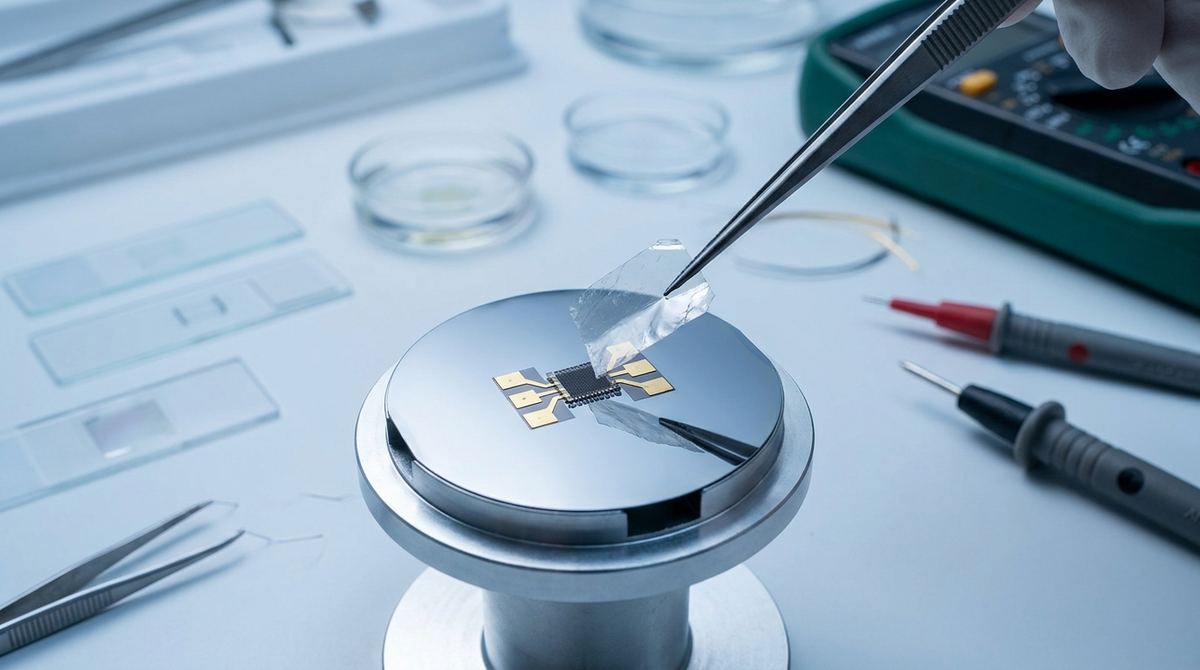
In the world of nanoelectronics and quantum materials, van der Waals (vdW) heterostructures are a cornerstone of innovation. By stacking atomically thin materials like graphene and hexagonal boron nitride (hBN), engineers can create devices with unique and powerful properties. However, a persistent challenge plagues the fabrication process: contamination.
The standard method for transferring and patterning these delicate 2D layers often involves polymers like polymethyl methacrylate (PMMA). While effective, these polymers inevitably leave behind residues on the material's surface. This contamination degrades device performance, introduces unpredictable behavior, and makes the surface unsuitable for highly sensitive characterization techniques like scanning tunneling microscopy (STM), which require pristine atomic surfaces. Removing these residues often requires aggressive cleaning or annealing processes that can damage the materials themselves.
A 2026 paper by Han Xuan Wong and colleagues, "Polymer-free Assembly of Unencapsulated van der Waals Heterostructure Devices," presents an elegant and practical solution. The researchers demonstrate that muscovite mica, a common layered mineral, can serve as a multi-functional, polymer-free platform for the entire device fabrication workflow. Mica can be used as a clean transfer stamp, a robust assembly support, and a removable shadow mask for patterning contacts.
This guide translates their research into a practical, step-by-step process for a small lab, university research group, or startup. We will walk through how to build a prototype three-terminal graphene/hBN device—a basic field-effect transistor (FET)—using this simplified, cleaner, and more accessible mica-based method.
The goal of this project is to construct a simple, unencapsulated graphene FET on a standard silicon substrate. This device will allow us to test the electrical properties of the graphene and confirm that our fabrication method is successful.
The final device structure will be:
1. Substrate/Back Gate: A silicon wafer with a layer of silicon dioxide (Si/SiO2). The highly doped silicon acts as the back gate to modulate the graphene.
2. Dielectric Layer: A thin flake of hexagonal boron nitride (hBN) placed on the SiO2.
3. Channel: A monolayer graphene flake placed on top of the hBN.
4. Contacts: Metal source and drain contacts deposited directly onto the graphene.
The key innovation we will employ is the mica-based technique from the source research. Instead of using polymers for transfer and photolithography or e-beam lithography for patterning, we will use carefully prepared flakes of mica for both steps. This approach dramatically reduces the potential for organic contamination and lowers the barrier to entry for fabricating high-quality vdW devices, as it bypasses the need for expensive lithography equipment. This makes it an ideal method for prototyping and fundamental research in graphene electronics.
This list includes the core components needed to build and test the device. While specialized equipment is required, this process avoids the need for a full-scale cleanroom and lithography setup.
Materials:
Substrates: Doped silicon wafers with a 285 nm or 300 nm thermally grown oxide layer. This oxide thickness provides good optical contrast for identifying monolayer graphene.
2D Material Sources:
High-purity natural graphite crystal.
High-purity hBN crystal.
The quality of your starting materials is critical. While this guide uses exfoliation from bulk crystals, the principles apply to devices made from high-quality turbostratic graphene flakes as well.
Mica: A sheet of high-quality muscovite mica.
Adhesives: Standard mechanical exfoliation tape (e.g., 3M Scotch tape or Nitto Denko dicing tape).
Solvents: High-purity acetone, isopropyl alcohol (IPA), and deionized (DI) water for cleaning substrates.
Contact Metals: High-purity gold (Au) pellets or wire (99.99%+) and an adhesion metal like chromium (Cr) or titanium (Ti).
Equipment:
Optical Microscope: A high-quality reflected light microscope with various magnifications (5x to 100x) is essential for identifying and aligning flakes.
Micromanipulator Stage: A precision XYZ stage, often integrated with the microscope, for manipulating the mica stamps and masks.
Hot Plate or Heated Stage: A stage with precise temperature control up to at least 150 °C.
Thermal Evaporator: A high-vacuum chamber for depositing metal contacts (e-beam or thermal).
Tube Furnace or Annealing Chamber: Capable of reaching at least 400 °C with a controlled atmosphere (high vacuum or inert gas like Argon).
Probe Station: For making electrical contact with the finished device.
Semiconductor Parameter Analyzer: An instrument like a Keithley 2400 or similar to apply voltages and measure small currents.
The mica tools are the heart of this process. You will prepare two types of tools from a single sheet of muscovite mica.
1. Use exfoliation tape to cleave the mica sheet, producing large, thin, and atomically flat flakes. You are looking for flakes that are a few square millimeters in area and appear transparent or have a faint color under the microscope.
2. Prepare the Pickup Stamp: Select a robust, clean mica flake and attach it to a carrier, such as a small piece of glass or a block of polydimethylsiloxane (PDMS). This will be your reusable tool for picking up and transferring the 2D material flakes.
3. Prepare the Shadow Mask: Select another thin mica flake. This flake will be used to define the shape of the metal contacts. The simplest mask is one with a long, atomically straight edge, which can be created by careful cleaving. You can place two such masks to define a channel. For more complex geometries, you might carefully cut or break the mica to create specific shapes, though this requires practice. The goal is to create a physical barrier that will block metal deposition in unwanted areas.
This step uses the standard mechanical exfoliation technique, a cornerstone of 2D material research.
1. Clean your Si/SiO2 substrates thoroughly by sonicating them in acetone, then IPA, and finally rinsing with DI water. Dry them with a nitrogen gun.
2. Take a piece of exfoliation tape and press it firmly onto your bulk graphite crystal.
3. Peel the tape off. You will see layers of graphite on the tape. Fold the tape onto itself and peel it apart several times to further thin the graphite layers.
4. Gently press the tape with the thinned graphite onto a clean Si/SiO2 substrate. Peel the tape away slowly and smoothly.
5. Repeat this process on a separate substrate using the hBN crystal.
6. Use your optical microscope to inspect the substrates. You are looking for monolayer graphene, which appears as a very faint, nearly transparent flake on 285-300 nm SiO2. Thin hBN flakes (10-30 nm thick) will have a more visible light pink or blue color. Identify and map the coordinates of several promising flakes of each material. For more background on material preparation, see our articles on graphene manufacturing techniques.
This is the critical transfer process described by Wong et al. It relies on temperature-dependent van der Waals forces.
1. Place the substrate with your target hBN flake on the heated microscope stage.
2. Using the micromanipulator, bring your mica pickup stamp down into contact with the hBN flake. Ensure full, even contact.
3. Heat the stage to 110-120 °C. The source research shows that pickup efficiency approaches 100% in this temperature range. The increased thermal energy enhances the adhesion between the mica and the hBN, making it stronger than the adhesion between hBN and the SiO2 substrate.
4. After holding at temperature for a minute, slowly retract the mica stamp. The hBN flake should cleanly lift off the substrate and adhere to your stamp.
5. Now, take your final target substrate, which contains the identified graphene flake, and place it on the stage. You may want to lower the stage temperature for the release step. An engineering assumption based on common practices is to use a temperature of 40-60 °C for stacking.
6. Carefully align the hBN flake (on the mica stamp) over the graphene flake.
7. Slowly bring the hBN into contact with the graphene.
8. Slowly retract the mica stamp. The hBN/graphene stack should now be fully assembled on the final substrate. The vdW attraction between the two 2D materials is strong enough to pull the hBN off the mica.
The beauty of this method is its simplicity and cleanliness. You have created a heterostructure with a pristine interface, free from any polymer or solvent exposure.
Although the transfer is clean, microscopic air bubbles or water molecules can get trapped between the layers during assembly. Annealing helps to remove these contaminants and ensures the layers are in perfect van der Waals contact.
1. Place your substrate with the assembled hBN/graphene stack into a tube furnace or vacuum chamber.
2. Evacuate the chamber to a high vacuum (e.g., 10^-6 Torr) or purge it with an inert gas mixture (a common choice is a mix of Argon and Hydrogen).
3. Slowly ramp up the temperature. The source paper refers to "mild thermal annealing." A cautious but effective starting point, based on standard practices in the field, is to anneal at 350 °C for 3-4 hours.
4. After the anneal, slowly ramp the temperature back down to room temperature before venting the chamber.
This step is crucial for achieving high electrical performance and creating a surface clean enough for advanced spectroscopic analysis.
Now we will define the source and drain contacts without any lithography.
1. Place the substrate back under the microscope with the micromanipulator.
2. Carefully pick up your prepared mica shadow mask and align it over the hBN/graphene stack. The mask should cover the central part of the graphene flake (the channel) while leaving the two ends exposed where you want to deposit the contacts.
3. Once aligned, gently lower the mask into contact with the surface. The vdW forces should be sufficient to hold the thin mica flake in place.
4. Carefully transfer the entire assembly (substrate + mask) into your thermal evaporator.
5. Pump the chamber down to a high vacuum.
6. Deposit the metal contacts. A standard recipe is to first deposit a 5 nm adhesion layer of Cr or Ti, followed by 50-80 nm of Au.
7. After deposition, vent the chamber and remove the sample.
8. Place the sample back under the microscope and use the micromanipulator or a fine pair of tweezers to carefully lift the mica mask off the surface. You should be left with two well-defined metal contacts on either end of your graphene channel.
The final step is to verify that your device functions as a transistor.
1. Mount the finished device on a probe station.
2. Using the probe manipulators, land one probe on the source contact, one on the drain contact, and make a third contact to the silicon substrate (this can be done by scratching away the oxide at the edge of the chip).
3. Connect the probes to your semiconductor parameter analyzer. The silicon is your gate, and the metal pads are your source and drain.
4. Apply a constant, small DC voltage between the source and drain (V_sd), for example, 20 mV.
5. Sweep the gate voltage (V_g) across a wide range, for example, from -50 V to +50 V, while measuring the current (I_sd) flowing between the source and drain.
6. Plot I_sd as a function of V_g. If the fabrication was successful, you should see a "V-shaped" transfer curve. The current will be at a minimum at a specific gate voltage, known as the Dirac point, and will increase as the gate voltage moves away from this point in either the positive or negative direction. This modulation of current with gate voltage is the defining characteristic of a field-effect transistor.
Transfer Failure: Flakes can tear or fail to pick up. This is often due to incorrect temperature or unclean surfaces. Mitigation: Calibrate your stage temperature carefully and ensure all substrates and tools are pristine. Practice the mechanical pickup motion until it is smooth.
Mask Slippage: The mica shadow mask can move during transport to the evaporator. Mitigation: Use the thinnest possible mica flake for the mask, as it will conform better to the surface. Handle the sample with extreme care.
Poor Contacts: High contact resistance can ruin device performance. Mitigation: Ensure the graphene surface is clean before masking and deposition. The post-assembly anneal is critical for this.
Material Quality: The performance of the final device is ultimately limited by the quality of the initial 2D crystals. Mitigation: Source high-quality materials and become proficient at identifying clean, defect-free flakes. Understanding graphene market research can help in sourcing reliable, high-grade materials.
This guide is based directly on the methods presented by Wong et al. (arXiv:2609.21120v1). The core concepts derived from the source are:
The use of muscovite mica as a polymer-free stamp for transfer.
The use of mica as a removable shadow mask for contact deposition.
The temperature-dependent pickup efficiency, with optimal pickup occurring around 110-120 °C.
The validation of the technique by fabricating a functional, gate-tunable graphene/hBN FET.
To make this guide practical, we have made the following engineering assumptions based on common laboratory practices:
Substrate: Si/SiO2 with 300 nm oxide.
Annealing Parameters: 350 °C for 3 hours in a high-vacuum or Ar/H2 environment.
Contact Metal Recipe: 5 nm Cr / 50 nm Au.
Testing Parameters: V_sd of 20 mV and a V_g sweep from -50 V to +50 V.
These parameters are excellent starting points, but you should expect to optimize them for your specific setup and materials. By following this mica-based approach, you can significantly simplify your vdW heterostructure fabrication process, enabling rapid prototyping and creating devices with exceptionally clean interfaces for next-generation electronic and quantum research.
Serious about B2B integration? Test our premium Pulsed Electrical Resistive Carbon Heating turbostratic graphene in your lab. 100g sample packs available now.
Explore More
Twisted trilayer graphene allows for remote electronic control of a decoupled layer, a breakthrough in moiré physics that could enable cleaner quantum devices.

New research reveals that graphene can accept energy from a 2D semiconductor in a highly selective, momentum-dependent way, paving the path for next-gen...

Explore how researchers are using graphene-based nanoplasmonic scintillators to tune light-matter interactions, paving the way for faster, more sensitive...