
Graphene Nanoplasmonics: Tuning Scintillators for Better Medical Imaging
Explore how researchers are using graphene-based nanoplasmonic scintillators to tune light-matter interactions, paving the way for faster, more sensitive...
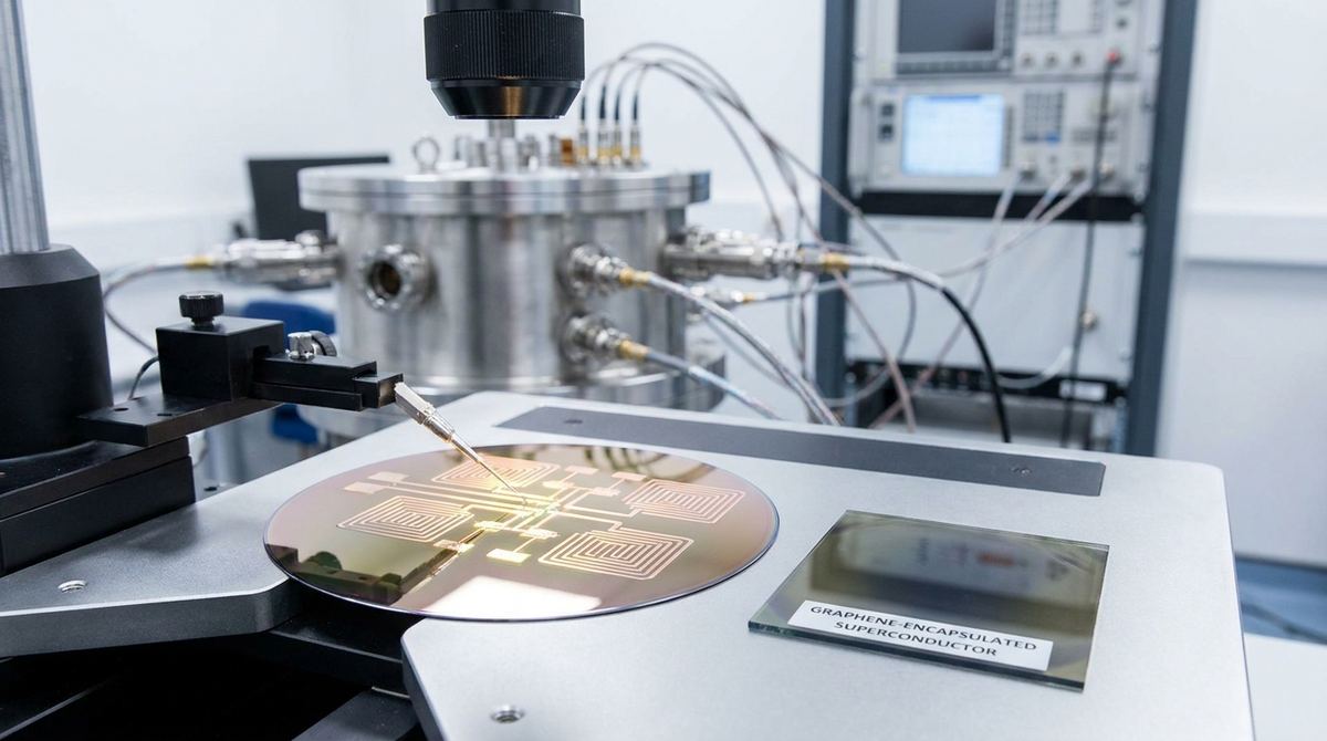
Two-dimensional (2D) superconductors are a frontier material for quantum information science. Their atomic thinness and pristine crystalline structure make them ideal candidates for creating the next generation of compact, high-performance quantum circuits and qubits. However, a significant barrier has prevented their widespread adoption: air. Most monolayer superconductors, like niobium diselenide (NbSe2), degrade almost instantly when exposed to oxygen and moisture, making fabrication and handling a nightmare reserved for labs with complex inert-atmosphere glovebox systems.
A 2026 research paper by Xudong Zheng, Jing Kong, and their colleagues introduces a groundbreaking technique called "encapsulation epitaxy." This method uses a layer of graphene not just as a protective shield but as an active template for growing a monolayer superconductor underneath it. The graphene is pre-deposited on a standard substrate, and the NbSe2 is grown beneath it, resulting in a perfectly encapsulated, air-stable heterostructure. This process transforms a fragile, lab-only material into a robust component that can be handled and processed using more conventional fabrication techniques.
This guide provides a practical walkthrough for a small lab, university research group, or advanced maker to replicate this concept. We will focus on building a single, crucial component for a superconducting quantum circuit: a high-kinetic-inductance inductor. This element is vital for creating compact resonators and certain types of qubits. By following these steps, you can fabricate a prototype device that leverages the unique properties of graphene-protected 2D superconductors.
The goal of this project is to fabricate and test a superconducting inductor made from a single atomic layer of niobium diselenide (NbSe2), protected by a monolayer of graphene. The final device will be patterned on a silicon-based substrate and will be designed for characterization at cryogenic temperatures.
The key innovation here is the air stability afforded by the graphene cap. This allows for the use of standard photolithography or e-beam lithography steps in a normal cleanroom environment, drastically lowering the barrier to entry for experimenting with 2D superconductors.
The inductor's performance is based on its kinetic inductance, a property derived from the inertia of superconducting charge carriers (Cooper pairs). In atomically thin materials like monolayer NbSe2, this inductance is exceptionally high, allowing for the creation of very compact circuit elements that would be much larger if made from conventional superconductors like aluminum or niobium. Our target is to achieve a kinetic inductance of approximately 0.7 nanohenries per square (nH/sq), as reported in the source research.
This is an advanced project requiring access to a cleanroom and specialized deposition and characterization equipment.
1. Substrates: 4-inch silicon wafers with a 300 nm thermal oxide layer (SiO2/Si) or a silicon nitride layer (Si3N4/Si). The source paper confirms both work.
2. Graphene: High-quality, large-area monolayer graphene grown via Chemical Vapor Deposition (CVD). The graphene should be transferred onto the final substrate before the superconductor growth step. Sourcing pre-transferred wafers is the most practical approach for a small lab. You can learn more about different graphene manufacturing techniques.
3. Superconductor Precursors: Metal-organic precursors for niobium and selenium suitable for Metal-Organic Chemical Vapor Deposition (MOCVD). For example, (tBuN)2(Me2N)2Nb and di-tert-butyl selenide (tBu2Se) are common choices, though the source paper does not specify the exact chemicals.
4. Carrier Gas: High-purity hydrogen (H2) and argon (Ar).
5. Lithography Chemicals: Photoresist or e-beam resist (e.g., PMMA), developer, and remover.
6. Contact Metal: Niobium titanium nitride (NbTiN) or another suitable superconductor for creating edge contacts. A sputtering target will be required.
7. Solvents: Acetone, isopropyl alcohol (IPA), and deionized water for cleaning.
1. MOCVD System: A furnace capable of reaching temperatures up to 800°C with precise gas flow and pressure control. This is the central piece of equipment for growing the NbSe2. Various types of industrial synthesis equipment are available, but a lab-scale reactor is sufficient.
2. Lithography System: An electron-beam lithography system is ideal for patterning the fine features of an inductor. A high-resolution photolithography setup can also be used for larger test structures.
3. Etching System: A Reactive Ion Etcher (RIE) with fluorine-based chemistry (e.g., SF6 gas) is needed to pattern the graphene/NbSe2 stack.
4. Sputtering System: For depositing the NbTiN contact pads.
5. Characterization Tools:
Atomic Force Microscope (AFM) for verifying surface morphology and layer thickness.
Raman Spectrometer for confirming the quality and integrity of the graphene and NbSe2 layers.
Cryogenic Probe Station or Dilution Refrigerator: Essential for testing the device at temperatures below the superconducting transition temperature (~1 Kelvin).
Low-Noise Electronics: Source-measure units (SMUs), lock-in amplifiers, and a Vector Network Analyzer (VNA) for electrical characterization.
This process follows the "encapsulation epitaxy" method. We will detail each stage, noting where we make engineering assumptions due to the limited detail in the source abstract.
Begin with a clean SiO2/Si substrate. The quality of this initial surface is critical for the subsequent growth.
1. Perform a standard RCA clean or a piranha etch on the wafer to remove organic and metallic contaminants.
2. Obtain a monolayer of CVD graphene on copper foil.
3. Use a wet transfer process to move the graphene from the copper foil to your SiO2/Si substrate. This typically involves spin-coating a support layer (like PMMA) on the graphene, etching away the copper, transferring the graphene/PMMA stack to the substrate, and finally dissolving the PMMA.
4. After transfer, anneal the substrate in a vacuum or Ar/H2 environment at around 300-400°C to remove residual polymer and improve the graphene-substrate interface. The result should be a uniform, large-area monolayer of graphene covering your substrate.
This is the core step of the process. The graphene-coated substrate is placed in an MOCVD reactor to grow the NbSe2 layer underneath the graphene.
1. Load the graphene/SiO2/Si substrate into the MOCVD chamber.
2. Purge the chamber thoroughly with high-purity argon.
3. Heat the substrate to the growth temperature. The source paper does not specify the exact temperature, which is a critical parameter you will need to optimize. A reasonable starting range for NbSe2 growth is 650°C to 800°C. We assume a starting point of 750°C.
4. Introduce the carrier gas, a mixture of Ar and H2.
5. Introduce the niobium and selenium precursors into the chamber at a controlled flow rate. The precursor molecules will diffuse through the graphene layer or its grain boundaries and react on the SiO2 surface, forming a monolayer of NbSe2. The graphene acts as a template, promoting epitaxial growth.
6. The growth duration will determine the film's quality and coverage. A starting point could be 15-30 minutes.
7. After growth, cool the system down slowly under an argon atmosphere. You now have a graphene/NbSe2/SiO2 heterostructure that is stable in ambient air.
Now, we use standard lithography to define the inductor shape. A meander-line pattern is a common choice for creating a compact, high-inductance element.
1. Spin-coat a layer of e-beam resist (e.g., PMMA A4) onto the graphene/NbSe2 surface.
2. Bake the resist according to the manufacturer's specifications.
3. Use an e-beam lithography system to write the inductor pattern into the resist. This involves selectively exposing the resist with an electron beam. The pattern should include the meander line itself and the areas for the contact pads.
4. Develop the resist in a suitable developer (e.g., a mixture of MIBK and IPA), which will wash away the exposed areas, leaving a resist mask on the substrate.
With the pattern defined, we etch away the unwanted material and create robust electrical contacts.
1. Place the patterned wafer into an RIE chamber.
2. Use a fluorine-based plasma, such as SF6 or CF4, to etch the exposed graphene/NbSe2 layers. The resist mask protects the inductor pattern. The underlying SiO2 acts as an etch stop.
3. After etching, remove the remaining resist mask with a solvent like acetone.
4. For the contacts, a second lithography step is required to define the contact pad areas. This process is similar to Step 3 but uses a different mask design.
5. The source paper highlights the importance of "superconducting edge-contacts." This involves ensuring a clean interface between the 2D material and the contact metal. Before depositing the contact metal, a gentle in-situ argon ion mill can be used to clean the edges of the patterned NbSe2.
6. Without breaking vacuum, deposit a layer of a 3D superconductor, such as 100 nm of NbTiN, using a sputtering system. This thicker superconductor ensures a low-resistance, superconducting connection to the monolayer device.
7. Perform a lift-off process by dissolving the resist. This removes the metal deposited on top of the resist, leaving behind only the desired contact pads connected to the edges of your NbSe2 inductor.
Verification involves both material and electrical characterization.
1. AFM: Before patterning, use an AFM to scan the surface of the graphene/NbSe2 film. You should see a uniform surface. The step height at the edge of the film should correspond to a single layer of NbSe2 (~0.7 nm) plus the graphene layer.
2. Raman Spectroscopy: Use a Raman spectrometer to confirm the material quality. You should see the characteristic G and 2D peaks for graphene. For monolayer NbSe2, you should observe the E2g and A1g vibrational modes. The absence of oxide-related peaks confirms the effectiveness of the graphene encapsulation.
This is the ultimate test of your device and must be performed at cryogenic temperatures.
1. Mount the device in a dilution refrigerator or a 3He cryostat capable of reaching temperatures below 1 K.
2. Resistance vs. Temperature (R-T): Perform a four-probe measurement of the inductor's resistance as you cool it down. You should observe a sharp drop in resistance to near-zero at the superconducting critical temperature (Tc). The source paper reports a Tc of approximately 1 K.
3. Kinetic Inductance Measurement: Measuring kinetic inductance directly is complex. A common method is to fabricate the inductor as part of an LC resonant circuit by adding a parallel capacitor.
Connect the resonator to a Vector Network Analyzer (VNA) via coaxial cables.
Measure the transmission (S21 parameter) through the circuit as a function of frequency. You will see a sharp dip at the resonant frequency, f0.
The kinetic inductance (LK) can be extracted from this resonant frequency using the formula f0 = 1 / (2π√(L_total C)), where L_total is the sum of the geometric and kinetic inductance. By designing the inductor to have a dominant kinetic inductance, you can calculate its value per square.
Expected Result: The source paper measured a kinetic inductance of ~0.7 nH/sq. This is significantly higher than conventional superconductors, confirming the value of the 2D material for compact quantum circuits.
This is a challenging project with several potential failure points.
Poor NbSe2 Growth: The growth under graphene may be non-uniform or incomplete. Mitigation: Systematically vary MOCVD parameters (temperature, pressure, precursor flow rates) on small test chips to find the optimal growth window.
Graphene Defects: Tears or wrinkles in the initial graphene transfer can act as sites for oxidation, compromising the entire device. Mitigation: Use high-quality CVD graphene and refine your transfer technique to be as gentle as possible. AFM and Raman scans can help identify defective areas to avoid during patterning.
High Contact Resistance: A poor connection between the NbTiN pads and the monolayer NbSe2 will ruin the device's performance. Mitigation: Adhere strictly to the edge-contact protocol. An in-situ cleaning step before contact deposition is crucial to remove any process-related residue or minimal oxidation at the edges.
Fabrication Damage: The monolayer materials are fragile and can be damaged during lithography or etching. Mitigation: Use optimized, low-power RIE recipes. Handle the wafers with care throughout the process.
This guide is based on the methods described in the 2026 arXiv preprint "Encapsulation epitaxy of air-stable monolayer superconducting films for quantum circuits and qubits" by Zheng et al. The core concept of growing NbSe2 under a graphene capping layer is taken directly from this work.
However, the source abstract does not provide a full recipe with all process parameters. The following are engineering assumptions and should be used as starting points for your own process development:
Exact MOCVD precursor chemicals, flow rates, pressure, and growth duration.
Specific lithography resist types and processing parameters (spin speeds, bake times).
RIE gas composition, flow rates, and power for the etching step.
The precise geometry and dimensions of the inductor test structure.
These parameters are highly dependent on the specific equipment used in your lab and will require careful calibration and optimization.
The potential for creating a wide range of air-stable 2D material heterostructures opens up new possibilities for device engineering. This technique could be applied to other sensitive materials, accelerating research and development in graphene electronics and quantum computing. By providing a practical pathway to fabricate robust devices, encapsulation epitaxy may be a key enabling technology for the future of quantum hardware.
Serious about B2B integration? Test our premium Pulsed Electrical Resistive Carbon Heating turbostratic graphene in your lab. 100g sample packs available now.
Explore More
Explore how researchers are using graphene-based nanoplasmonic scintillators to tune light-matter interactions, paving the way for faster, more sensitive...

Researchers discover a moiré heterostructure with a unique "dual-flatness" electronic property, enabling continuous electrical tuning between exotic quantum...

Explore chiral fermion localization in two-kink systems. This theoretical physics research offers a powerful new model for controlling electrons in...