
Practical Guide: Build a Graphene FET with a Polymer-Free Mica Transfer Method
Learn a practical, polymer-free method for building a graphene FET using muscovite mica for clean transfer, assembly, and contact patterning.
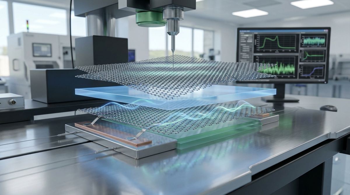
Imagine being able to change the fundamental properties of a material just by bringing another one nearby, without them ever touching. This isn't science fiction; it's the cutting edge of condensed matter physics, where the strange quantum rules that govern the world of atoms and electrons allow for remarkable new forms of control. By carefully stacking and twisting atom-thin sheets of carbon, scientists are discovering ways to create custom electronic landscapes. This ability to precisely engineer a material's behavior is the foundation for the next generation of computing, sensing, and communications technology. A recent breakthrough in this field demonstrates a new, more elegant way to achieve this control, opening a door to cleaner and more versatile electronic devices.
In the world of materials science, pristine monolayer graphene is a superstar. It is a single sheet of carbon atoms arranged in a honeycomb lattice, and its unique structure allows electrons to move through it at incredible speeds as if they have no mass. This makes it an exceptional conductor. However, for use in digital electronics like computer chips, a material needs to act as a semiconductor, meaning it must have an "off" switch—a way to stop the flow of electrons. This is known as having a bandgap. Creating a reliable bandgap in graphene without ruining its amazing conductivity has been a central challenge for over a decade.
A powerful technique that emerged to solve this is called "twistronics." By stacking two layers of graphene and twisting one slightly relative to the other, a beautiful interference pattern called a moiré superlattice emerges. This pattern creates a new, larger-scale periodic landscape that profoundly alters the material's electronic properties, including opening up the coveted bandgap. The problem is that this process directly couples the two graphene layers. Their electronic systems merge, which can introduce complexities, unwanted interactions, and a susceptibility to tiny imperfections in the stacking. This makes it difficult to study and control the properties of one layer independently of the other. The research conducted by Dohun Kim, Junsik Choe, Takashi Taniguchi, Kenji Watanabe, Gil Young Cho, and Youngwook Kim addresses this fundamental limitation. They sought a way to harness the power of a moiré pattern to control a graphene layer without the drawbacks of direct physical and electronic coupling.
The central innovation of this work is the concept of "remote modulation." Instead of creating a complex, intertwined system, the researchers designed a structure that uses one part of the device as a remote control for another. They built a three-layer graphene stack with a specific architecture. The top two layers were twisted to create a standard moiré pattern. This twisted bilayer acts as the "control" unit. The third, bottom layer of graphene is the "active" unit, the one whose properties they want to manipulate.
Crucially, they separated the top twisted pair from the bottom monolayer with an ultrathin insulating sheet of hexagonal boron nitride (hBN). This insulator acts as a barrier, preventing electrons from hopping between the top and bottom sections. The two graphene systems are therefore physically and electronically "decoupled." The key insight is that while electrons cannot cross the barrier, the electric field generated by the moiré pattern in the top layers can. This field extends through the insulator and imprints a "ghost" of the moiré pattern onto the bottom layer. This remote influence gently modulates the electronic landscape of the bottom layer, changing its properties in a predictable way, all while leaving the layer itself pristine and isolated.
The device is a van der Waals heterostructure, meaning it is built by stacking different two-dimensional materials on top of one another, held together by weak van der Waals forces. The specific stack, from top to bottom, consists of twisted bilayer graphene (TBG), a few layers of hexagonal boron nitride (hBN), and a single layer of monolayer graphene (MLG). The TBG on top is created with a precise, small twist angle between its two graphene sheets. This small rotation is what generates the moiré superlattice, a periodic potential that dictates the behavior of electrons within the TBG.
The hBN layer is a critical component. It is an excellent electrical insulator with an atomic structure very similar to graphene, making it an ideal, atomically smooth substrate and separator. Its role here is to act as a dielectric spacer, a barrier that stops electrons from tunneling between the TBG control unit and the MLG active unit. The thickness of this hBN layer is carefully chosen to be thin enough for the electric field from the TBG to penetrate effectively, yet thick enough to ensure robust electronic isolation.
The bottom MLG is the target of the experiment. In its natural state, its electrons obey the physics of a "Dirac cone," which describes their massless, high-mobility behavior. The experiment's goal is to see if the periodic electric field emanating from the top TBG can create a new superlattice potential in this isolated MLG. If successful, this would fundamentally alter the MLG's electronic band structure, imprinting the moiré pattern's characteristics onto it without any physical contact or electronic hybridization. This approach could lead to new types of graphene electronics where the control and active regions are cleanly separated.
Through a combination of sophisticated measurement techniques, the team confirmed their hypothesis. They used scanning tunneling microscopy (STM) to directly visualize the atomic and electronic structure of the device. Their measurements showed that the bottom graphene layer, despite being separated by the hBN insulator, exhibited a clear electronic modulation that matched the periodicity of the moiré pattern from the top twisted bilayer. This was the first direct evidence of remote moiré modulation.
Furthermore, they performed quantum transport measurements, which analyze how electrons flow through the material in response to electric and magnetic fields. These tests revealed the emergence of secondary Dirac points in the electronic band structure of the bottom monolayer graphene. These new features are a textbook signature of a superlattice potential at work. Their appearance confirmed that the remote electric field was strong enough to create a new, engineered electronic landscape in the target layer.
Crucially, the transport data also confirmed that the two subsystems remained decoupled. The electronic signatures of the top twisted bilayer and the bottom monolayer were distinct and did not show signs of hybridization or interlayer tunneling. The bottom layer behaved like a pristine sheet of graphene subjected to a perfectly periodic external electric field, just as the researchers had intended. This successful demonstration of remote control over a decoupled Dirac system represents a significant advance in the field of twistronics.
This discovery introduces a powerful new degree of freedom for designing quantum materials and devices. By separating the source of the moiré potential (the TBG) from the active material (the MLG), engineers can avoid many of the problems associated with directly coupled twisted systems. The active layer can remain electronically "clean," free from the structural defects, strain, and electronic complexities that can arise in a twisted interface. This is analogous to the difference between mixing two chemicals together versus using one to influence the other through a glass wall; the latter provides control without contamination.
This principle of decoupling could lead to more reliable and higher-performance devices. For example, in a transistor, this could allow for the creation of a pristine conducting channel whose properties are tuned by a remote, patterned "gate," potentially leading to lower scattering and higher electron mobility. For quantum computing applications, maintaining the coherence of quantum states is paramount. A decoupled system like this could protect fragile quantum information in the active layer from disturbances in the control layer, a critical step toward building more robust qubits. The ability to "imprint" a potential onto a material opens up a new paradigm for materials engineering on demand.
While this research is a landmark proof of principle, it is important to recognize its current limitations. The devices were fabricated using mechanical exfoliation, a meticulous laboratory technique that is not suitable for large-scale manufacturing. Developing methods for creating such precise, multi-layer stacks over large areas is a major engineering hurdle that must be overcome for commercialization. The challenges of scalable production are a significant focus in the industry, driving innovation in graphene manufacturing techniques.
The experiments were also performed under cryogenic temperatures and in a high-vacuum environment to minimize thermal noise and environmental interference. Further research is needed to determine how robust this remote modulation effect is at room temperature and under more practical operating conditions. The strength of the remote potential is also dependent on the thickness and dielectric properties of the insulating barrier. A thicker barrier provides better isolation but a weaker effect. Optimizing this trade-off for different applications will require extensive further study. Finally, researchers will need to explore a wider range of twist angles and material combinations to fully map out the possibilities of this new technique.
Although commercial products based on this specific finding are likely many years away, the long-term implications are profound. The ability to engineer the band structure of a clean, decoupled 2D material could revolutionize semiconductor technology. It offers a path toward creating highly tunable graphene-based transistors, photodetectors, and modulators for next-generation computing and high-speed communications. The fine control over the electronic landscape could also be used to create novel metamaterials with exotic optical or thermal properties.
In the realm of quantum technologies, this work is particularly exciting. The creation of perfectly periodic potentials is essential for trapping and manipulating electrons to form artificial atoms or quantum dots, which are building blocks for quantum computers. The clean platform provided by remote modulation could be ideal for creating arrays of identical, stable qubits. The principles demonstrated here could also extend beyond graphene to other 2D materials, opening up a modular, "plug-and-play" approach to designing a vast array of quantum heterostructures for various graphene applications.
Researchers have successfully used the electric field from a twisted graphene bilayer to remotely control the electronic properties of a separate, underlying graphene layer. This was achieved through a thin insulating barrier, demonstrating that a moiré pattern's influence can be transmitted without direct contact, paving the way for cleaner and more versatile quantum devices.
What is a moiré pattern in graphene?
A moiré pattern is a large-scale interference effect that appears when two similar repeating patterns, like the hexagonal lattices of graphene sheets, are overlaid with a slight angle or mismatch between them. In twisted graphene, this creates a new, much larger "superlattice" that dramatically changes how electrons move through the material, introducing novel electronic behaviors like superconductivity or insulating states that are not present in a single graphene sheet.
What are decoupled Dirac subsystems?
In this context, "Dirac subsystems" refers to the distinct electronic systems of the different graphene layers, where the electrons behave according to the Dirac equation for relativistic, massless particles. "Decoupled" means that these electronic systems are isolated from each other by an insulating barrier. Electrons cannot easily move between the layers, so the properties of one layer can be preserved in a pristine state even while being influenced by the other.
Why is it important that the layers are decoupled?
Decoupling the control layer from the active layer is critical for creating high-performance electronic devices. When layers are directly coupled, imperfections and electronic "noise" from one layer can interfere with the other, degrading performance. By keeping them separate, the active channel remains electronically clean and undisturbed, which can lead to higher electron mobility, less signal scattering, and more reliable and predictable device operation, a crucial factor for both classical and quantum computing.
What is twisted trilayer graphene?
Twisted trilayer graphene is a stack of three atomic layers of graphene. The specific configuration in this research involves a twisted bilayer of graphene placed on top of a single monolayer of graphene, with an insulating sheet in between. This structure is engineered to use the top twisted pair as a source of a moiré potential to influence the bottom, isolated monolayer, creating a highly controlled and complex quantum system.
Is this technology ready for commercial use?
No, this technology is in the early, fundamental research stage. It represents a significant scientific discovery, demonstrating a new physical principle for controlling materials at the nanoscale. However, major engineering and manufacturing challenges, such as developing scalable fabrication methods and ensuring robust operation at room temperature, must be solved before this concept can be translated into commercial products.
The work on remote moiré modulation in twisted trilayer graphene marks a conceptual leap forward in the field of quantum materials. By demonstrating that the powerful effects of a moiré superlattice can be projected across an insulating barrier, researchers have unlocked a new method for device engineering. This principle of decoupling the control and active components allows for the creation of cleaner, more pristine electronic systems, addressing a key challenge in the quest to build next-generation electronics. While the path from this laboratory discovery to industrial application is long, the fundamental insight it provides will undoubtedly inspire new designs for quantum computers, ultra-efficient transistors, and novel sensors, further solidifying graphene's role as a cornerstone material for future technology.
Serious about B2B integration? Test our premium Pulsed Electrical Resistive Carbon Heating turbostratic graphene in your lab. 100g sample packs available now.
Explore More
Learn a practical, polymer-free method for building a graphene FET using muscovite mica for clean transfer, assembly, and contact patterning.

New research reveals that graphene can accept energy from a 2D semiconductor in a highly selective, momentum-dependent way, paving the path for next-gen...

Explore how researchers are using graphene-based nanoplasmonic scintillators to tune light-matter interactions, paving the way for faster, more sensitive...