Imagine if we could shrink the components of a laser or an optical sensor down to the size of a single atom. For over a century, engineers have been fighting against the diffraction limit, a fundamental rule of physics that says you cannot focus light into a space much smaller than its own wavelength. This limitation is a massive roadblock for the next generation of ultra-fast computers and tiny medical sensors. However, a new frontier in material science is offering a way out. By stacking incredibly thin, two-dimensional materials like graphene, scientists can create hybrid particles that behave in ways light alone never could. This research, led by Daeho Noh, Jaehyeong Ock, Sergey G. Menabde, and Min Seok Jang, explores how these engineered materials can split the very nature of light and vibration, opening a door to unprecedented control over light at the nanoscale.
The Problem This Research Is Solving
The core challenge in modern photonics is the scale of interaction. Most traditional optical devices, like those found in fiber-optic cables or standard lasers, rely on light waves that are hundreds of nanometers in size. While this is fine for long-distance communication, it is far too bulky for the nanoscale world of modern transistors and microchips. If we want to integrate light into the circuitry of a computer chip, we need a way to squeeze that light into much smaller volumes.
The problem is that light, in its pure form, is difficult to confine. It naturally wants to spread out. To force light into a tiny space, we have to rely on the interaction between light and matter. Even when we use surface waves, we are often limited by the physics of how those waves move through a single material. In standard materials, the way light moves—its dispersion—is fixed by the chemical properties of that material. This leaves engineers with very few knobs to turn if they want to change how light behaves. To create the next generation of nanophotonic devices, we need a way to fundamentally change the relationship between energy and momentum for these light-matter particles, and standard bulk materials simply do not offer enough flexibility.
The Key Idea in Plain English
The breakthrough idea involves a concept called hybridization. In the world of physics, when two different types of waves—like a wave of light and a wave of atomic vibration—meet in a very small space, they can sometimes merge into a single, new kind of particle. This new particle is called a polariton.
Think of it like two dancers moving through a ballroom. If they move independently, they might cross paths for a split second and then continue on. But if they are deeply connected, they might start moving in sync, creating a new, complex dance routine that neither could perform alone. In the research conducted by Noh, Ock, Menabde, and Jang, the scientists are looking at how stacking different 2D materials allows us to force light and atomic vibrations to dance together. When this interaction becomes strong enough, it causes a phenomenon called dispersion splitting. This is essentially a mathematical and physical "break" in the path of the waves. Instead of the waves crossing through each other, they push each other away, creating new energy levels that did not exist before. This "splitting" is the key to engineering entirely new optical properties that are not found in nature.
How the Graphene-Based System Works
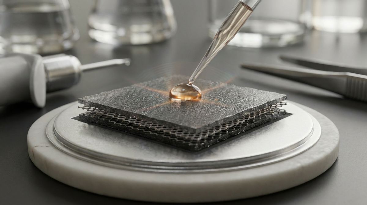
To achieve this level of control, the researchers utilized van der Waals heterostructures. These are essentially "atomic sandwiches" made by stacking layers of different materials, such as graphene and hexagonal Boron Nitride (hBN), on top of one another. These layers are held together by van der Waals forces, which are much weaker than the chemical bonds found inside a single crystal, but they are strong enough to keep the stack stable.
The system works through the interplay of two distinct types of waves. First, there are surface plasmon polaritons (SPPs). These occur when light interacts with the free electrons in a conductive material like graphene. Because graphene is a superb conductor with very high electron mobility, it can support these waves, which are highly confined to the surface of the material. Second, there are phonon polaritons (PhPs). These occur when light interacts with the vibrations of the ions in a crystal lattice, such as the lattice in boron nitride.
When these two layers are stacked closely together, the electromagnetic field generated by the moving electrons in the graphene reaches out and "feels" the vibrating ions in the boron nitride layer. This is the coupling mechanism. Because the layers are only a few atoms thick, the interaction is incredibly intense. The electric field of the plasmonic mode couples with the oscillating dipole moments of the lattice vibrations. This interaction is what drives the system into the "strong coupling regime," where the two waves can no longer be thought of as separate entities. They become a single, hybrid system where the energy and momentum of the waves are fundamentally altered by the presence of the other.
What the Researchers Found
The primary finding of this research is the observation and characterization of dispersion splitting within these heterostructures. In physics, a dispersion curve is a map that shows how the energy of a particle relates to its momentum. For a single material, this map is usually a smooth, continuous line. However, when the coupling between the plasmon and the phonon becomes strong enough, the two curves do not simply cross each other.
Instead, they experience what is known as anticrossing. As the energy levels of the plasmon and the phonon approach one another, the interaction forces the curves to bend away from each other. This creates a "gap" or a "split" in the dispersion relation. This splitting is a direct physical manifestation of the strength of the interaction. The larger the gap, the more effectively the light and matter are coupled.
The researchers found that by carefully choosing the materials and the thickness of the layers in the van der Waals stack, they could precisely tune this splitting. This means they can effectively "program" the dispersion of the polaritons. By controlling the splitting, they can manipulate the group velocity of the waves—essentially deciding how fast the light-matter particle moves through the material—and the confinement of the wave, deciding how tightly it is squeezed. This provides a level of tunability that is impossible in bulk crystals or single-layer materials.
Why the Result Matters
The ability to engineer dispersion splitting is a massive leap forward for nanophotonics. For decades, scientists have been looking for ways to create "metamaterials"—materials that have properties not found in nature—at the atomic scale. This research shows that van der Waals heterostructures are a perfect platform for this because they are inherently tunable.
When we can control dispersion, we can control the very fundamental properties of how information is carried by light. If we can manipulate the way waves move through a material, we can create ultra-compact waveguides that bend light around sharp corners without loss. We can create nanolasers that are much smaller and more efficient than current technology. Most importantly, we can create highly sensitive sensors. Because the dispersion splitting is so sensitive to the environment, even a single molecule landing on the surface of the heterostructure could shift the splitting, creating a measurable change in the optical signal. This could lead to a new generation of diagnostic tools that can detect diseases at the molecular level instantly.
Limitations and What Still Needs Testing
While the results are scientifically groundbreaking, it is important to understand that this technology is currently in the fundamental research phase. The fabrication of van der Waals heterostructures is an incredibly delicate process. Currently, many of these structures are made using mechanical exfoliation—essentially peeling layers off a crystal with adhesive tape—and stacking them manually under controlled environments. This process is highly precise but is currently impossible to scale for mass manufacturing. For this to become a commercial reality, we need reliable, large-scale manufacturing techniques like chemical vapor deposition (CVD) that can produce these atomic sandwiches over large areas with perfect alignment.
Furthermore, the behavior of these polaritons can be sensitive to temperature. While some modes are stable at room temperature, many of the most interesting quantum effects occur at cryogenic temperatures to minimize thermal noise from the lattice. For practical applications like consumer electronics, these effects must be robust enough to operate in a standard operating environment. Finally, the research focuses on the theoretical and simulated dispersion splitting; transitioning from these theoretical models to actual, functional integrated photonic circuits will require significant engineering efforts to manage loss and signal degradation.
Real-World Applications
The implications for real-world technology are vast and span several industries. In the field of telecommunications, these materials could lead to on-chip optical interconnects. Currently, computers transfer data using electrical signals through copper wires, which generate heat and limit speed. Replacing these with light-based signals on a chip would increase bandwidth and reduce power consumption significantly.
In the medical field, as mentioned earlier, the sensitivity of these polaritonic states could revolutionize point-of-care diagnostics. A chip made of these heterostructures could act as a highly sensitive scale, detecting the presence of specific proteins or viral particles by observing the shift in their dispersion splitting.
In the realm of computing, these findings could contribute to the development of optical computing or neuromorphic computing. If we can use light to perform computations at the nanoscale, we could potentially create processors that are orders of magnitude faster than current silicon-based chips, while using a fraction of the energy.
If You Remember One Thing
If you remember only one thing from this research, let it be this: by stacking two-dimensional materials, we can force light and matter to merge into new particles, allowing us to manipulate light at scales far smaller than its own wavelength.
FAQ
What is a phonon polariton? A phonon polariton is a quasiparticle that arises when light interacts with the vibrations of atoms within a crystal lattice. This interaction binds the photon to the phonon, creating a new entity that carries both electromagnetic and mechanical characteristics. This allows light to be controlled at much smaller scales than is possible with light alone.
Why are van der Waals heterostructures used for this? Van der Waals heterostructures allow scientists to stack different materials like LEGO bricks. Because the layers are held together by weak forces rather than rigid chemical bonds, we can combine materials that wouldn't normally go together. This gives us a high degree of control over the electronic and optical properties of the final stack.
What does dispersion splitting actually mean? Dispersion refers to how the energy of a wave changes with its momentum. When two waves interact strongly, they "repel" each other's energy levels, creating a gap where no wave can exist. This splitting is a direct signal that the light and matter are behaving as a single, unified system.
Can graphene be used for more than just this? Yes, graphene is a highly versatile material. Beyond its role here in creating hybrid polaritons, it is used in everything from flexible touchscreens to high-speed transistors and advanced battery electrodes due to its incredible conductivity and surface area.
What is the diffraction limit and why is it a problem? The diffraction limit is a physical boundary that prevents light from being focused into a spot smaller than roughly half its wavelength. This is a problem because it prevents us from making optical components (like lenses or waveguides) as small as electronic components, which limits how much we can shrink our technology.
Conclusion
The work of Daeho Noh, Jaehyeong Ock, Sergey G. Menabde, and Min Seok Jang represents a significant step forward in our ability to master the nanoscale. By leveraging the unique properties of van der Waals heterostructures, they have demonstrated how dispersion splitting can be used to engineer the interaction between light and matter. While challenges in manufacturing and environmental stability remain, the ability to manipulate light-matter particles through atomic stacking provides a clear pathway toward the next generation of ultra-fast, ultra-small, and ultra-sensitive optical technologies.