Imagine if you could change the color of a laser beam simply by passing it through a microscopically thin film. In the world of classical physics, light behaves in predictable ways, reflecting off surfaces or passing through glass. But there is a more advanced realm called nonlinear optics, where light can be forced to interact with itself and its environment to create entirely new frequencies. This is not just science fiction; it is the fundamental principle behind how we might one day process information using light instead of electricity. By manipulating the very structure of materials at the atomic scale, scientists are learning how to "repackage" light, turning one color into another with incredible precision.
The Problem This Research Is Solving
Current technology relies heavily on silicon-based electronics, which move electrons through circuits to perform calculations. However, as we demand faster speeds and lower power consumption, we are hitting the physical limits of how much heat these electrons generate. Light, or photons, offers a solution because photons do not generate heat in the same way electrons do, and they can travel at much higher frequencies. The challenge is that most natural materials are not good at changing the frequency of light efficiently. To achieve nonlinear optical effects, like changing the frequency of light, we typically need very thick, expensive, and bulky crystals. These bulky components are incompatible with the tiny, integrated chips used in modern smartphones and computers. There is a desperate need for a new class of materials that can perform these complex optical transformations at the nanoscale, within a footprint no larger than a few atoms.
The Key Idea in Plain English
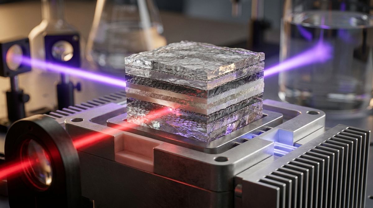
The solution lies in the creation of metamaterials made from van der Waals layers. Think of these materials as the ultimate Lego set for physicists. Instead of having a single solid block of material, we can stack incredibly thin, two-dimensional sheets on top of one another. These sheets can be different types of materials, and by stacking them in specific ways, we can create "designer" properties that do not exist in nature. The research explores using topological insulators within these stacks. These are special materials that act as insulators in their bulk but have highly conductive surfaces. Because these surface states are topologically protected, they are incredibly robust and predictable. By combining these unique electronic properties with the stacking ability of van der Waals materials, we can create a metamaterial that is specifically tuned to change the frequency of light through a process called harmonic generation.
How the Graphene-Based System Works
To understand how this system works, we must look at the interaction between electromagnetic waves and the electronic structure of the material. When light hits a material, its oscillating electric field pushes and pulls on the electrons. In standard materials, this response is linear, meaning the electrons move in a way that directly mirrors the light wave. However, in the van der Waals metamaterials studied by the researchers, the structure is engineered to produce a nonlinear response.
The mechanics of this process depend heavily on the symmetry of the atomic arrangement. In these materials, the van der Waals force acts as a weak "glue" that holds the individual layers together without creating strong chemical bonds. This allows us to maintain the unique electronic properties of each layer while controlling the overall symmetry of the entire stack. For example, second harmonic generation, or SHG, occurs when two photons are absorbed and one photon is emitted at twice the original frequency. This process is highly sensitive to symmetry; specifically, it requires the material to lack inversion symmetry. If the atoms are arranged in a perfectly symmetrical way, SHG is forbidden. However, by stacking different layers or twisting them, we can intentionally break that symmetry.
Third harmonic generation, or THG, is a different beast. It involves three photons merging to create one photon with triple the frequency. Unlike SHG, THG can occur even in materials that are perfectly symmetrical. The research focuses on how the specific electronic states of topological insulators—specifically those surface states where electrons behave like massless particles—contribute to these effects. The conductivity and the specific way the electrons are distributed at the interfaces between the van der Waals layers determine how efficiently the material converts the light. By controlling the thickness of the layers and the nature of the interfaces, we can tune the material to be an efficient producer of either SHG or THG light.
What the Researchers Found
The study conducted by Alessandra Di Gaspare, Sara Ghayeb, Craig Knox, Edmund H. Linfield, Joshua Freeman, and Miriam S. Vitiello provides deep insights into how these topological insulator-based metamaterials behave under intense light. The researchers analyzed how the different harmonic orders—SHG and THG—respond to the specific crystalline structure of the van der Waals stack. They found that the nonlinear optical response is not just a property of the material itself, but a property of how the layers are organized.
A key finding involves the relationship between the symmetry of the material and the intensity of the harmonic signals. The research demonstrated that by carefully selecting the topological insulator and the stacking sequence, it is possible to manipulate the ratio between second and third harmonic generation. This is a massive deal because it means we can use these materials as "optical filters" or "frequency converters" that are highly selective. Furthermore, the study explored how the electronic properties of the topological insulator's surface states enhance these nonlinear processes. Because the surface electrons are so uniquely controlled by the material's topology, they provide a highly efficient pathway for the light-matter interaction that drives harmonic generation. The results suggest that these metamaterials can act as highly precise tools for light manipulation at the atomic scale.
Why the Result Matters
The implications of this research are profound for the future of photonics and information technology. If we can reliably engineer materials that convert frequencies through harmonic generation at the nanoscale, we move one step closer to the dream of all-optical computing. In an all-optical computer, information would be processed using light pulses rather than electrical currents. This would allow for massive increases in processing speed and a significant reduction in the energy required to run data centers.
Beyond computing, this research matters because it provides a blueprint for "on-chip" optical components. Currently, if a scientist needs to change the wavelength of a light source, they might need an entire room full of lasers and crystals. This research suggests a future where that same function is performed by a single, ultra-thin layer of material integrated directly onto a microchip. This could revolutionize medical imaging, where compact, high-frequency light sources are needed for deep-tissue scanning, or telecommunications, where light-based signals need to be converted rapidly to handle the massive amounts of data moving across the internet.
Limitations and What Still Needs Testing
While the findings are exciting, it is important to note that this technology is still in the fundamental research phase. The research describes the physical principles and the observed behaviors in a controlled setting, but it does not describe a commercially ready product. One of the primary limitations is the complexity of fabrication. While van der Waals stacking is powerful, creating perfect, defect-free stacks of atomic layers is incredibly difficult and difficult to scale for mass production.
Additionally, the stability of these materials under continuous exposure to high-intensity light remains a question for future study. Nonlinear optical processes often require high-intensity light to be efficient, and there is always a risk that such intense energy could damage the delicate atomic structure of the metamaterial over time. Furthermore, the research focuses heavily on the theoretical and experimental physics of the materials; how these materials would behave when integrated into a complex, multi-component electronic circuit has yet to be fully explored. We need to understand how the thermal properties and the mechanical stresses of a real-world device might affect the precise symmetry required for these optical effects.
Real-World Applications
The potential real-world applications for topological insulator-based metamaterials are vast and diverse. In the field of sensing, these materials could lead to the development of ultra-sensitive detectors capable of identifying specific chemical signatures by observing how they shift the frequency of light passing through the material. This could revolutionize environmental monitoring and security screening.
In the realm of telecommunications, these materials could enable the development of next-generation optical modulators. As we move toward 6G and beyond, the ability to manipulate light at higher frequencies and with higher precision will be essential for handling the massive bandwidth requirements of a hyper-connected world. Additionally, in the field of quantum computing, the ability to control light with extreme precision is vital for the manipulation of quantum bits, or qubits, which may rely on single photons for information transfer. These metamaterials could provide the necessary interface between traditional electronic circuits and quantum optical systems.
If You Remember One Thing
If you take away only one concept from this research, let it be this: the ability to control the frequency of light by engineering the atomic symmetry of stacked 2D materials is a transformative step toward ultra-fast, low-power optical technology.
FAQ
What is harmonic generation in simple terms?
Harmonic generation is a process where light interacts with a material and comes out as a different color. If you shine a red light into a material and it comes out blue, it has undergone a frequency change. This happens because the light waves interact with the electrons in the material in a way that forces them to oscillate at a multiple of the original frequency.
Why are topological insulators considered special for this research?
Topological insulators are unique because they are insulators on the inside but have highly conductive paths on their surface. These surface paths are "protected" by the laws of physics, meaning electrons can move along them without being easily scattered by defects. This predictable and robust electronic behavior makes them excellent candidates for controlling how light interacts with the material.
What makes van der Waals materials so useful for engineers?
Van der Waals materials are essentially two-dimensional sheets that can be stacked like thin layers of paper. This allows scientists to create "metamaterials" with custom-made properties. By changing how these layers are stacked or even by twisting them, we can create materials with optical or electrical properties that do not exist in nature.
Can these materials replace current silicon chips?
It is unlikely they will replace silicon entirely, but they are likely to complement it. While silicon is excellent for much of our current computing, light-based (photonic) systems are better suited for high-speed communication and certain types of processing. We are likely looking at a future of "hybrid" systems where silicon and optical metamaterials work together.
Is this technology available for consumer use today?
No, this research is currently in the fundamental science stage. The researchers are working to understand the physics and prove the concepts in a laboratory environment. Transitioning from a laboratory experiment to a mass-produced component in a smartphone requires significant advances in manufacturing and long-term stability testing.
Conclusion
The study of second and third harmonic generation in topological insulator-based van der Waals metamaterials represents a significant leap forward in our ability to manipulate light. By leveraging the unique symmetry-breaking properties of these layered structures, researchers like Alessandra Di Gaspare and her colleagues are opening new pathways for optical engineering. While challenges in manufacturing and material stability remain, the ability to control light frequency at the atomic scale holds the promise of a new era in high-speed, energy-efficient, all-optical technology.