
Graphene-Silicon Modulator Unlocks High-Speed Data at New Wavelengths
Explore a breakthrough graphene-silicon slot-waveguide modulator. This high-speed device operates at both 1.5 μm and 2 μm, promising next-gen optical networks.
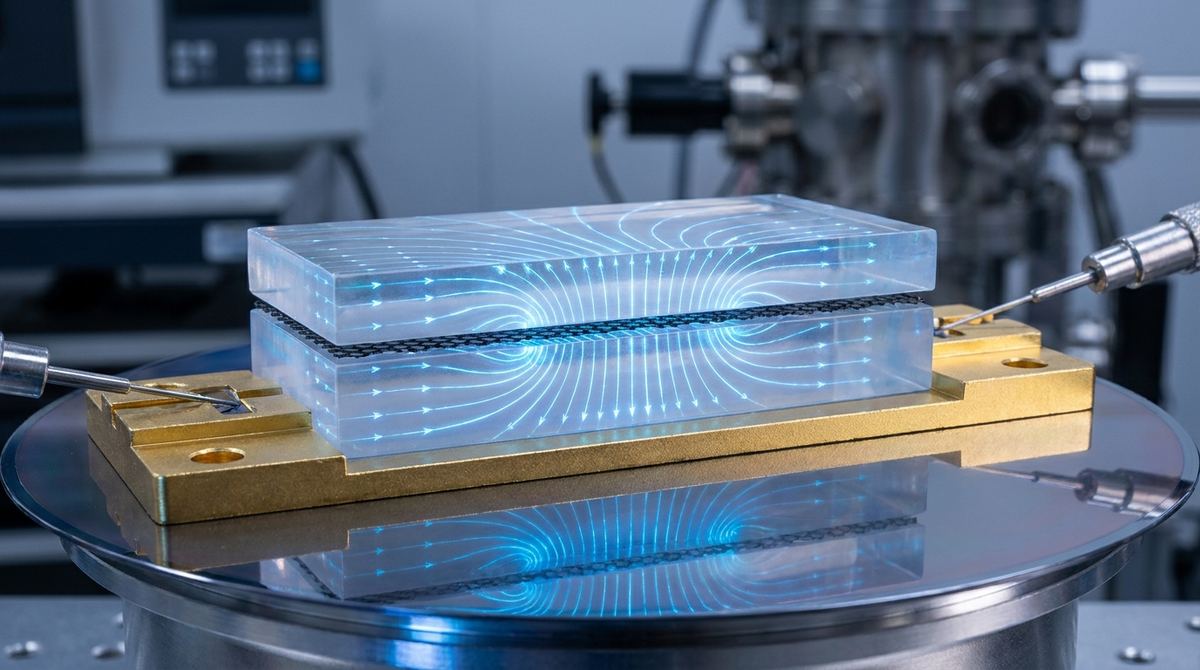
For engineers and startups working on next-generation semiconductor devices, the Graphene Field-Effect Transistor (GFET) represents a massive opportunity for high-speed, low-power electronics. However, simulating these devices accurately presents a significant computational hurdle. The primary difficulty lies in the extreme scale mismatch between the graphene layer and the surrounding dielectric oxides.
In a standard GFET, you have a two-dimensional material—graphene—sandwiched between two three-dimensional oxide layers. Traditional Finite Element Methods (FEM) require a mesh that conforms to the geometry of the device. Because the graphene layer is only one atom thick, creating a high-quality mesh that captures the physics at the interface without becoming computationally impossible is a nightmare. If the graphene layer is slightly non-planar or the interface is irregular, you are forced to remesh the entire system every time you change the geometry.
This guide outlines how to move away from traditional meshing and toward an unfitted ghost-FEM approach to model the electrostatic potential and charge transport in GFETs. This method allows you to simulate the device on a fixed Cartesian grid, making it much easier to handle the complex interfaces between the oxide and the graphene.
The research by Astuto and Nastasi provides a breakthrough for engineers by utilizing an unfitted ghost finite element method. Instead of trying to force a mesh to fit the graphene layer, this method uses level-set functions to represent the geometry. This means you can keep a simple, fixed grid regardless of how complex the interface becomes.
Key technical advantages for the engineer include:
1. Geometry Flexibility: You can model irregular or rough interfaces without the need for expensive remeshing.
2. Interface Accuracy: By using a symmetric Nitsche formulation, the method weakly enforces the interface conditions, ensuring that the transition between the oxide and the graphene is captured with high precision.
3. Computational Efficiency: The use of a snapping-back-to-grid strategy helps manage the small-cut-cell issues that typically plague unfitted methods, preventing numerical instability.
For a startup or a small lab, this means you can run much more complex simulations of device variations—such as thickness fluctuations or gate voltage effects—without spending weeks on manual mesh preparation.
Because the specific dimensions of a device vary depending on the fabrication process, you will need to define your own parameters. Based on standard GFET architectures, the following are cautious starting ranges for your simulation models.
Graphene Layer:
The thickness should be modeled as a single layer, approximately 0.34 nm. While the research suggests that the effective thickness and discretization affect the transverse potential profile, for initial modeling, a single-layer approximation is the standard.
Dielectric Oxide:
Commonly silicon dioxide (SiO2) or high-k dielectrics like Hafnium Oxide (HfO2).
Thickness range: 20 nm to 300 nm.
Dielectric constant (k): 3.9 for SiO2; 25 for HfO2.
Charge Transport:
The model should utilize a self-consistent drift-diffusion-Poisson model. For the graphene layer, use a one-dimensional bipolar drift-diffusion equation in the degenerate case.
Electrical Parameters:
Gate Voltage (Vg): -5V to +5V.
Drain-Source Voltage (Vds): 0V to 5V.
Carrier Mobility (mu): This is highly dependent on the substrate. For a SiO2 substrate, assume a range of 1000 to 5000 cm2/Vs.
Temperature:
Standard room temperature (300K) is the recommended starting point for all simulations.
To build a predictive model for your GFET prototype, follow this computational workflow.
Step 1: Geometry Definition via Level-Sets
Define your oxide/graphene/oxide structure using level-set functions. This allows you to define the boundaries of the graphene layer as an interface rather than a physical mesh boundary. This is essential for capturing the transverse potential profile accurately.
Step 2: Physics Coupling
Set up the coupled nonlinear system. You must solve the Poisson equation for the electrostatic potential across the entire three-layer structure. Simultaneously, you must solve the drift-diffusion equations for the charge transport within the graphene layer.
Step 3: Interface Enforcement
Apply the symmetric Nitsche formulation to the interface between the oxide and the graphene. This ensures that the electric field and the potential are continuous (or follow the required jump conditions) across the interface without needing a conforming mesh.
Step 4: Numerical Solving
Use a damped fixed-point iteration to solve the coupled system. To manage the three-layer geometry efficiently, implement a domain-decomposition treatment. This breaks the problem into smaller, manageable pieces (oxide 1, graphene, oxide 2) and solves them iteratively until convergence.
Step 5: Data Extraction
Extract the transfer characteristics (Id-Vg curves). Look for the transition from the OFF state to the ON state to verify that your model correctly predicts the device's switching behavior.
A simulation is only useful if it matches reality. Once your model is built, follow this validation plan:
1. Benchmark Validation: Before applying the model to your specific device, test it against standard elliptic interface benchmarks. Verify that you achieve second-order accuracy for the solution and first-order accuracy for the gradient.
2. Transfer Characteristic Comparison: Compare your simulated Id-Vg curves against experimental data from your lab's fabrication process. If the transition from OFF to ON is not sharp, re-examine your mobility model and the discretization of the graphene layer.
3. Transverse Potential Check: Use the simulation to visualize the electrostatic potential across the thickness of the device. This will help you understand how the gate voltage influences the carrier distribution within the graphene.
While this method is powerful, engineers should be aware of the following risks:
Computational Complexity: While you save time on meshing, the unfitted ghost-FEM approach requires sophisticated numerical solvers. The damped fixed-point iteration can be computationally intensive if the grid is extremely fine.
Parameter Sensitivity: The model is highly sensitive to the mobility model used. If your graphene mobility is significantly different from your assumption (due to substrate impurities or grain boundaries), your simulated transfer characteristics will not match your physical device.
Dimensionality Assumptions: The research indicates that the effective thickness of the graphene layer affects the transverse potential profile. If your application requires extreme precision in the vertical electric field, you cannot treat the graphene as a simple 2D sheet; you must use a full two-dimensional electrostatic description.
Source Basis: This guide is based on the research findings of Astuto and Nastasi (2026) regarding second-order unfitted ghost-FEM for elliptic interface problems applied to low-dimensional semiconductor devices.
Serious about B2B integration? Test our premium Pulsed Electrical Resistive Carbon Heating turbostratic graphene in your lab. 100g sample packs available now.
Explore More
Explore a breakthrough graphene-silicon slot-waveguide modulator. This high-speed device operates at both 1.5 μm and 2 μm, promising next-gen optical networks.

New research reveals that mechanical strain doesn't just reduce but fundamentally reshapes heat flow in graphene, a critical insight for flexible...

Learn to build a gate reflectometry sensor using bilayer graphene. This practical guide details a non-contact method for material characterization.