
Atomic-Scale Visualization of Antiferromagnetic Bit Switching in 2D Materials
Researchers have directly observed Néel vector switching in a single-layer antiferromagnet, Cr2S3, at the atomic scale, a breakthrough for future spintronic...
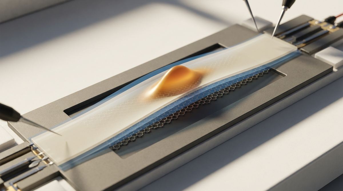
To build the next generation of supercomputers or quantum processors, scientists must first master the art of prediction. We cannot simply build every possible version of a new material to see if it works; instead, we must simulate the behavior of electrons with incredible precision. At the heart of this simulation challenge lies the difficulty of describing where an electron is and how it moves within a complex crystal lattice. When electrons are modeled as waves spreading across an entire material, the math becomes incredibly complex and computationally expensive. This research represents a major step forward in how we represent these tiny, energetic particles, allowing us to create much clearer and more efficient digital models of the materials that will power our future.
In the realm of quantum mechanics, electrons in a solid-state material like graphene do not behave like tiny billiard balls. Instead, they behave like waves that are spread across the entire crystal. This is described by something called Bloch waves. While Bloch waves are mathematically perfect for describing the overall state of the material, they are notoriously difficult to use when we want to look at specific, local details. For example, if a scientist wants to understand how a single defect in a graphene sheet affects the movement of electrons, or how a specific chemical bond interacts with a neighboring atom, the wave-like nature of Bloch waves becomes a computational nightmare. Because the electron is "everywhere" at once in the model, the mathematical matrices required to solve these problems become massive and incredibly difficult for even the most powerful supercomputers to process.
The fundamental issue is known as the gauge freedom problem. In quantum mechanics, the phase of a wave is somewhat arbitrary. You can change the phase of an electron's wave function without changing the actual physical reality of the electron, but this change in phase completely transforms the mathematical description of the electron. If the phase is not handled with extreme care, the resulting mathematical functions become "delocalized," meaning they spread out across the entire material. When functions are spread out, the computational cost of simulating the material sky-rockets because every part of the system becomes mathematically linked to every other part. To make simulations efficient and accurate, scientists need to find a way to "localize" these functions—to force the mathematical description to focus on a specific, tiny area around an atom, much like a spotlight rather than a floodlight. These specialized, localized functions are known as Maximally Localized Wannier Functions.
The breakthrough proposed by Yuji Hamai and Katsunori Wakabayashi involves a method to "shape" these localized electron packages using a process called discrete adiabatic transport. To understand this, imagine you are trying to guide a delicate object through a series of moving obstacles. If you move too quickly or erratically, you will lose control and the object will collide with something. However, if you move very slowly and smoothly, following the natural curves of the environment, you can guide the object precisely to a target. This is the essence of "adiabatic" movement.
In the context of quantum modeling, the researchers are not moving a physical object, but rather moving the mathematical "phase" of the electron wave. They have found a way to navigate the complex mathematical landscape of electron states by taking small, discrete steps. By moving through these steps carefully—what we call adiabatic transport—they can gradually refine the shape of the electron functions. This process essentially "squeezes" the electron wave until it is as compact and localized as possible. By doing this, they turn the overwhelming "floodlight" of a Bloch wave into a highly precise "spotlight" (the Wannier function) without losing the essential quantum information that defines the material.
While this research is a mathematical and computational advancement, its application to systems like graphene is where its true utility lies. In a material like graphene, the electrons exist in a unique two-dimensional plane with very specific energy levels. The system works by taking the existing, delocalized Bloch states—which are the standard starting point for any quantum simulation—and applying the discrete adiabatic transport method to them.
The process begins by defining the movement through momentum space, which is the mathematical space where we track the properties of waves. Instead of trying to solve the localization problem all at once, which is mathematically overwhelming, the researchers use a discrete approach. They divide the journey from a spread-out wave to a localized function into a series of tiny, manageable steps. At each step, the mathematical function is slightly adjusted to minimize its spread. Because the movement is "adiabatic," the function stays in its most stable and efficient state throughout the transformation.
This transformation is critical for materials like graphene because the electronic properties of 2D materials are highly sensitive to the geometry and the "topology" of the electron's path. The researchers' method ensures that as the function is being shaped, the fundamental topological characteristics—the "knots" and "twists" in the electron's wave-like structure—are preserved. This ensures that the localized Wannier function isn't just a simple approximation, but a mathematically rigorous representation that still contains all the complex quantum physics of the original material.
Through their theoretical work, Yuji Hamai and Katsunori Wakabayashi have demonstrated that discrete adiabatic transport is a robust method for constructing these maximally localized functions. Their approach allows for the creation of Wannier functions that are highly accurate even in systems with very complex electronic structures. The research shows that by navigating the mathematical landscape in discrete, controlled steps, one can overcome the errors that often plague other methods of localization.
Crucially, the researchers found that this method is capable of handling the complexities introduced by the "gauge" of the wave functions. Because the method is designed to follow the evolution of the system smoothly, it avoids the mathematical "jumps" or errors that occur when one tries to force a wave into a localized shape too abruptly. This leads to the creation of Wannier functions that are more "maximally localized" than what previous techniques could achieve. In the language of computational physics, this means the resulting mathematical matrices are much "sparser," which is a technical way of saying they are much easier and faster for a computer to solve.
The importance of this research lies in the bridge it builds between high-level quantum theory and practical material engineering. Currently, there is a massive bottleneck in materials science: the time and cost required to simulate new materials. If a company is trying to develop a new type of semiconductor for a faster smartphone chip, they might need to simulate thousands of different atomic configurations. If each simulation takes weeks of supercomputer time, the pace of innovation is slowed.
By providing a more efficient way to create Wannier functions, this research enables much faster and more accurate simulations. When the mathematical functions are highly localized, the computer doesn't have to calculate the interactions between every single atom and every other atom in a massive block of material; it only needs to calculate the interactions between nearby atoms. This reduction in complexity allows scientists to simulate larger systems, more complex interfaces, and more realistic defects. This, in turn, leads to faster discovery of new materials and more reliable predictions of how a device will perform before it is ever manufactured in a factory.
It is important to clarify that this research is a development in computational methodology, not a physical discovery of a new material. The work of Hamai and Wakabayashi provides a new tool for the toolbox of the materials scientist; it does not, by itself, create a new type of graphene or a new semiconductor. The method is a mathematical framework used to improve the accuracy of simulations.
Furthermore, while the method is efficient, the "discrete" nature of the transport still requires significant computational resources. The precision of the result depends heavily on the number of steps taken during the adiabatic transport. While the method is much better than previous approaches, the trade-off between the number of steps (which increases accuracy) and the computational time (which increases cost) remains a critical factor for researchers to manage. Future testing will likely focus on how this method performs in extremely large-scale systems, such as complex biological molecules or highly disordered materials, where the complexity of the electronic landscape might challenge even the most robust adiabatic transport models.
The practical implications of improved quantum modeling are vast and touch almost every area of modern technology. In the semiconductor industry, this method can be used to design more efficient transistors that operate at higher frequencies with less heat generation. As we reach the physical limits of traditional silicon-based electronics, the ability to accurately model new materials like transition metal dichalcogenides or topological insulators becomes essential for the next leap in computing power.
In the field of quantum computing, the ability to simulate the behavior of qubits (quantum bits) with high precision is the holy grail. Many quantum computing architectures rely on very specific electronic states that are highly sensitive to their environment. The ability to use maximally localized Wannier functions to model these states could help engineers design more stable qubits and more effective error-correction protocols. Additionally, in the development of high-efficiency solar cells and advanced battery chemistries, the ability to model how electrons move across interfaces and through defects can lead to the discovery of materials that capture more energy or store more power than current technologies.
If you take away only one idea from this research, let it be this: the ability to accurately and efficiently model the "local" behavior of electrons is the key to unlocking the next generation of advanced materials. By using discrete adiabatic transport to shape electron wave functions into compact, localized packages, researchers are providing the mathematical precision needed to design the future of electronics, quantum computing, and sustainable energy.
What is a Wannier function and why is it used? A Wannier function is a mathematical way of describing an electron that is focused on a specific location in a crystal, rather than being spread out across the entire material. Scientists use them because they make the math much simpler and faster for computers to solve, especially when we want to study how local features like defects or individual atoms affect the material.
How does "adiabatic transport" work in this context? In physics, "adiabatic" refers to a process that happens so slowly and smoothly that the system stays in its most stable state. In this research, it means moving the mathematical phase of an electron wave through a series of small, careful steps so that the resulting function is shaped perfectly without losing any important quantum information.
Does this research mean we have a new material? No, this research is about a new mathematical method used to study materials. It is a way to make our computer simulations of materials like graphene much more accurate and much faster, which helps scientists design better materials in the future.
Why is it important to have "localized" functions? When mathematical functions are spread out across a whole material, they are computationally "heavy" and slow to process. When they are localized, the math becomes "sparse," meaning the computer only has to focus on the most important local interactions. This drastically reduces the time and power needed to run complex quantum simulations.
How does this affect the future of technology? By making simulations more accurate and efficient, this method helps speed up the development of new technologies. This includes faster computer chips, more stable quantum computers, and more efficient energy storage solutions like better batteries and solar cells.
The work of Yuji Hamai and Katsunori Wakabayashi represents a vital advancement in the computational toolkit of modern physics. By solving the mathematical challenges associated with the localization of electron wave functions, they have paved the way for more efficient and precise simulations of quantum materials. As we move toward an era defined by quantum technologies and highly specialized advanced materials, the ability to "shape" our mathematical models with such precision will be indispensable. This research ensures that our ability to simulate the microscopic world keeps pace with our ambition to engineer it.
Serious about B2B integration? Test our premium Pulsed Electrical Resistive Carbon Heating turbostratic graphene in your lab. 100g sample packs available now.
Explore More
Researchers have directly observed Néel vector switching in a single-layer antiferromagnet, Cr2S3, at the atomic scale, a breakthrough for future spintronic...

A new physics-informed AI method reconstructs the 3D atomic structure and dynamics of graphene from a single low-dose TEM image, solving a key imaging...

Explore how to build a graphene-FGT voltage-tuned microwave filter. This guide details a prototype for electrically controlling magnetic damping in spintronics.