
3D Atomic Imaging of Graphene Dynamics from a Single Low-Dose TEM Snapshot
A new physics-informed AI method reconstructs the 3D atomic structure and dynamics of graphene from a single low-dose TEM image, solving a key imaging...
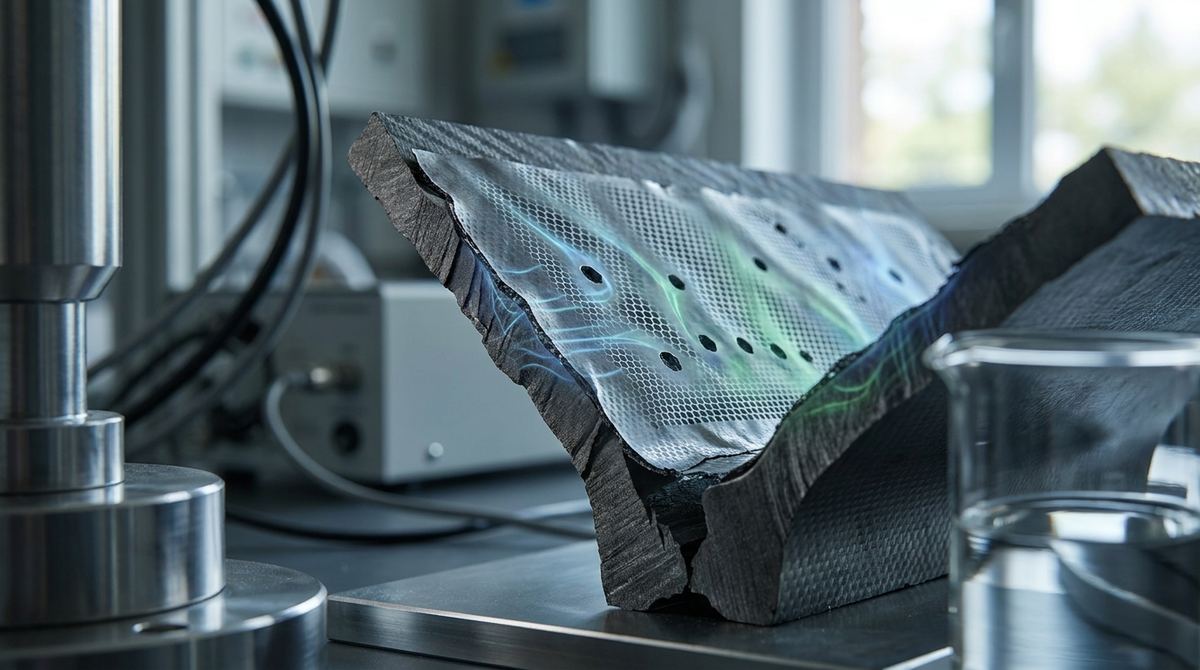
Imagine a world where electronic signals do not scatter or dissipate into heat, but instead flow along indestructible, predefined paths, much like water following a perfectly carved riverbed. This is not science fiction, but the reality of topological physics. In traditional materials, electrons are like chaotic crowds in a busy city, constantly bumping into obstacles, which generates heat and slows down devices. However, by fundamentally changing the geometry of the material, scientists can force electrons into highly organized, protected patterns. This research into the periodic behavior of topology in graphene with nanohole arrays explores how we can "program" the very nature of electricity by simply changing the physical pattern of a material.
As the world pushes for faster computing and more efficient energy storage, the limitations of traditional silicon-based electronics are becoming increasingly apparent. In standard semiconductor materials, the movement of electrons is subject to scattering. This scattering occurs when electrons collide with impurities, defects, or the vibrating atoms of the material itself. These collisions lead to electrical resistance, which manifests as heat. Heat is the enemy of modern technology; it limits how much power we can pump into a chip before it melts and creates noise that interferes with delicate electronic signals.
Furthermore, as we attempt to shrink transistors to the atomic scale, the "messiness" of electron movement becomes a major hurdle. At these tiny scales, the probabilistic and chaotic nature of electron scattering makes it difficult to maintain consistent performance. We need a way to create electronic pathways that are "topologically protected." In physics, topology refers to properties that remain unchanged even if the material is slightly deformed or if there are small imperfections. If we can create a material where the electronic states are topologically protected, we can ensure that electrons follow specific lanes regardless of minor manufacturing defects or heat, leading to near-zero loss and unprecedented efficiency.
The solution proposed by Yong-Cheng Jiang, Xing-Xiang Wang, and Xiao Hu involves introducing a deliberate, organized pattern of "obstacles" into the graphene sheet. Instead of relying on random impurities, which cause unpredictable scattering, they suggest using a nanohole array. Think of a perfectly smooth floor versus a floor with a very precise, repeating pattern of small divots. On the smooth floor, a ball might roll anywhere, but on the patterned floor, the ball is forced into specific tracks dictated by the arrangement of the divots.
By punching a regular array of tiny holes into a layer of graphene, we create what is known as a superlattice. This superlattice acts as a new master template that overrides the natural movement of the electrons. The research focuses on how the arrangement and spacing of these holes—the periodicity—dictates the topological nature of the electrons. Essentially, the researchers are looking for a way to tune the material so that it flips between different topological states just by adjusting the geometry of the holes. This would allow engineers to "switch" the properties of a material without changing its chemical composition, simply by changing its physical pattern.
To understand how this works, we must look at the unique structure of graphene. Graphene is a single layer of carbon atoms arranged in a hexagonal lattice. Its electrons behave like "massless Dirac fermions," meaning they move at incredibly high speeds, similar to light, and follow a very specific mathematical rule called the Dirac equation. In its pristine state, graphene has a unique property where its conduction and valence bands meet at a single point, known as the Dirac point. This makes graphene highly conductive but also makes it difficult to create a "band gap," which is essential for turning transistors off.
When we introduce a nanohole array, we are essentially imposing a new periodicity onto the carbon lattice. This new periodicity creates a "superlattice potential." In the world of quantum mechanics, when you introduce a periodic potential, you transform the electronic energy landscape. The original Dirac cones of the graphene are modified, creating "mini-bands." These mini-bands are much smaller than the original electronic bands and are highly sensitive to the geometry of the holes.
The holes act as local disruptions to the electronic wavefunctions. Because the holes are arranged in a repeating, periodic pattern, these disruptions aren't random; they are synchronized. This synchronization causes the electron wavefunctions to acquire a specific mathematical property called the Berry phase. The Berry phase is a global property that describes how the phase of a wave changes as it moves through a cycle in momentum space. When the nanohole array is structured correctly, the Berry phase accumulates in a way that forces the electronic bands to take on non-trivial topological characteristics. This is where the "topology" comes in: the holes are not just holes; they are the architects of the electron's path.
The study conducted by Jiang, Wang, and Hu reveals a fascinating phenomenon: the topological properties of the graphene-nanohole system are periodic. This means that as you change the parameters of the holes—such as their size or the distance between them—the topological state of the material does not just change randomly. Instead, it cycles through different phases.
The researchers discovered that the Chern number, which is a mathematical value that identifies the topological state of a system, fluctuates in a predictable, repeating manner as the lattice constant of the nanohole array is tuned. This is a significant finding because it proves that the topological behavior is a direct consequence of the structural periodicity. By varying the ratio of the hole diameter to the lattice spacing, the system can transition from a "trivial" state (where electrons behave normally and are prone to scattering) to a "topological" state (where electrons move in protected, quantized channels).
This periodic behavior suggests that there is a "map" of topological states available for graphene. Depending on where you set the hole spacing, you can place the material into a specific electronic regime. This ability to cycle through states through geometric tuning is the core breakthrough described in the research. It moves the field from simply observing topological effects to actively designing and predicting them through structural engineering.
The implications of this research are profound for the future of condensed matter physics and materials science. First, it provides a theoretical framework for "topological band engineering." Currently, creating topological insulators often requires using complex, exotic materials that are difficult to work with. This research shows that we can achieve similar, highly controlled results using graphene—a material that is already widely studied and potentially scalable—simply by adding a geometric layer of complexity.
Second, the periodic nature of the topology means we have a level of control that was previously unachievable. If we know that a specific hole spacing produces a specific topological phase, we can manufacture graphene sheets with customized electronic properties. This would allow for the creation of "programmable matter," where the electronic functionality is defined by the physical architecture of the material's surface.
Finally, this research bridges the gap between structural engineering and quantum physics. It demonstrates that the way we physically shape a material at the nanoscale can fundamentally rewrite its quantum mechanical laws. This opens up a new design space for scientists: instead of searching for new chemicals, we can look for new geometries.
While these findings are theoretically significant, it is important to distinguish between a mathematical model and a physical device. The research presented is a theoretical exploration of the periodic behavior of topology. It provides a roadmap, but it does not present a finished product.
One of the primary challenges is the precision required for fabrication. To achieve the predicted topological states, the nanoholes must be placed with atomic-scale precision. Any deviation from the periodic pattern—caused by manufacturing errors or unevenness in the graphene sheet—could introduce "disorder." In topological physics, too much disorder can destroy the very protection that makes the material useful, causing the electronic states to collapse.
Furthermore, the scale of these effects is often observed in computational models or at extremely low temperatures. For these topological states to be useful in a smartphone or a laptop, they must be stable at room temperature. Current research often focuses on the fundamental physics of how these states emerge, but the transition from a theoretical model to a room-temperature, commercially viable device remains a significant hurdle that requires extensive experimental validation and advanced manufacturing techniques like electron-beam lithography or helium-ion milling.
The ability to control electron topology through geometry suggests several revolutionary applications. In the realm of quantum computing, topological protection is a "holy grail." Quantum bits (qubits) are notoriously fragile and prone to errors caused by environmental noise. If we can use topological graphene to create "topologically protected qubits," we could create quantum computers that are much more stable and much easier to scale.
In the field of ultra-low-power electronics, this research could lead to a new class of "topological transistors." Unlike current transistors that rely on moving electrons through resistive channels, a topological transistor could move electrons through protected edge states. This would drastically reduce the heat generated by electronic devices, potentially leading to computers that are significantly faster and more energy-efficient than today's best silicon chips.
We may also see developments in high-sensitivity sensors. Because the topological states are so sensitive to the underlying geometry and external fields, a graphene nanohole array could be used to detect incredibly small changes in pressure, temperature, or chemical presence, making them ideal for advanced medical diagnostics or environmental monitoring.
If you take away only one concept from this research, let it be this: geometry is destiny for electrons. By using precise patterns of nanoholes, we can move beyond the chaotic, heat-generating movement of electrons and instead engineer predictable, indestructible pathways for electricity to follow.
Question: What exactly is "topology" in the context of this research?
Answer: In physics, topology refers to properties of a system that stay the same even if the system is slightly stretched or bent. When we talk about the topology of electrons in graphene, we are talking about how their quantum states are organized in a way that makes them "robust" or "protected" against small errors or defects in the material.
Question: Why is graphene the preferred material for this kind of study?
Answer: Graphene is uniquely suited for this because its electrons behave like massless particles, moving at very high speeds. This unique electronic structure makes it incredibly sensitive to geometric changes, meaning that adding a pattern of holes has a much more dramatic and controllable effect on the electrons in graphene than it would in a standard material like silicon.
Question: What is the role of the "nanohole array" in this process?
Answer: The nanohole array acts as a superlattice, which is a new, larger-scale pattern imposed on the existing carbon atoms. This array creates a new set of rules for how electrons move, forcing them into specific energy bands and allowing scientists to manipulate their topological properties by simply changing the size or spacing of the holes.
Question: Does this mean we will have topological computers soon?
Answer: Not immediately. This research is a fundamental scientific study that proves the theory works. Moving from this theoretical proof to a working device requires overcoming massive engineering challenges, such as making the holes with perfect precision and ensuring the effects work at room temperature rather than in a laboratory freezer.
Question: How does this help reduce heat in electronic devices?
Answer: Heat is caused by electrons bumping into things and losing energy. In a topological state, the electrons are forced into "protected" paths where they cannot easily be scattered by impurities or defects. Because they don't "bump" into things as much, they lose much less energy to heat, making the whole system more efficient.
The work of Yong-Cheng Jiang, Xing-Xiang Wang, and Xiao Hu marks a significant step forward in our ability to command the behavior of electrons. By demonstrating that the topological properties of graphene can behave periodically in response to a nanohole array, they have shown that we can use geometric patterns to "program" the quantum properties of a material. This intersection of geometry and quantum mechanics offers a powerful new toolkit for engineers and physicists, promising a future where electronic components are more robust, more efficient, and fundamentally controlled by the very shape of the materials from which they are built.
Serious about B2B integration? Test our premium Pulsed Electrical Resistive Carbon Heating turbostratic graphene in your lab. 100g sample packs available now.
Explore More
A new physics-informed AI method reconstructs the 3D atomic structure and dynamics of graphene from a single low-dose TEM image, solving a key imaging...

Explore how to build a graphene-FGT voltage-tuned microwave filter. This guide details a prototype for electrically controlling magnetic damping in spintronics.

Researchers map ballistic transport in bilayer graphene junctions, revealing quantized conductance thresholds. This fundamental work is key to designing...