
Practical Guide: Prototyping a Graphene Nanoribbon Photodetector
Build a near-infrared photodetector with nitrogen-doped porous graphene nanoribbons. This guide details the materials, fabrication steps, and test plan.
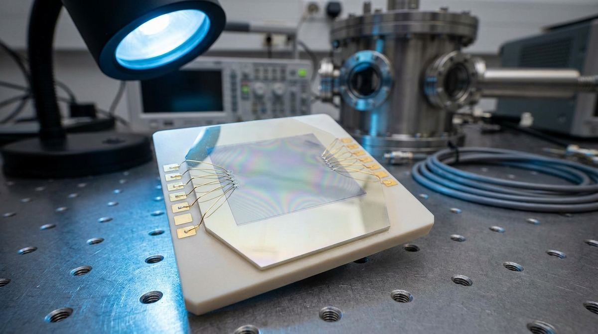
In high-radiation environments—such as medical radiotherapy rooms, particle accelerators, or space applications—standard silicon-based sensors face rapid degradation. Radiation induces charge trapping and lattice defects that cause sensor drift, eventually leading to total device failure. For engineers developing dosimetry tools (devices that measure radiation dose), the goal is to create a sensor that remains stable even after exposure to mega-gray (MGy) levels of radiation.
Recent research into electrostatic interface engineering suggests that graphene-based sensors, when paired with a hexagonal boron nitride (h-BN) spacer, can solve this problem. By carefully tuning the ratio between graphene's quantum capacitance and the device's geometric capacitance, we can suppress the resonance shifts that typically ruin sensor accuracy. This guide outlines how to approach the prototyping of a graphene-assisted MR-DWELL (Magneto-Resonant Dosimeter) using these principles.
The stability of this graphene sensor relies on the relationship between two types of capacitance:
1. Quantum Capacitance (Cq): This is an intrinsic property of the graphene layer, related to the density of states.
2. Geometric Capacitance (Cg): This is determined by the physical thickness and dielectric constant of the h-BN spacer layer.
In a standard sensor, radiation-induced charges shift the chemical potential of the graphene, causing the sensor signal to drift. However, by adjusting the thickness of the h-BN layer, we can control the screening factor. When the quantum capacitance is properly balanced against the geometric capacitance, the device becomes much less sensitive to these radiation-induced shifts. According to the research, this tuning can suppress resonance shifts by a factor of three and allow the device to maintain 83 percent of its peak current even after a 1 MGy dose.
To prototype this device, you will need high-quality 2D materials and precision fabrication tools.
Materials:
- Graphene: CVD-grown graphene on a copper or polymer substrate is most practical for scaling.
- Hexagonal Boron Nitride (h-BN): High-quality, atomically flat flakes or thin films.
- Substrate: Silicon with a thick thermal oxide layer (SiO2/Si) is a standard starting point.
- Electrodes: Titanium (Ti) for adhesion and Gold (Au) for high conductivity.
- Encapsulation: A thin layer of Al2O3 or PMMA to protect the device from environmental moisture.
Equipment:
- Electron-beam lithography (EBL) system or high-resolution photolithography.
- Thermal evaporator or sputtering system for metal deposition.
- Atomic Force Microscope (AFM) for thickness verification.
- Semiconductor Parameter Analyzer (e.g., Keithley) for electrical characterization.
- Lock-in amplifier for second-derivative spectroscopy.
The following steps describe the assembly of a graphene-hBN heterostructure. Note that these steps assume a standard cleanroom environment.
1. Substrate Preparation: Clean the SiO2/Si substrate using a standard RCA clean or oxygen plasma to ensure a pristine surface.
2. h-BN Deposition: Deposit the h-BN spacer layer. While the research does not specify a universal thickness, an engineering assumption for a balanced screening factor would be a thickness between 2 nm and 10 nm. For a first prototype, start with 5 nm of h-BN.
3. Graphene Transfer: Use a polymer-assisted transfer method (such as the PMMA method) to place the CVD graphene onto the h-BN layer. It is critical to ensure no bubbles or trapped air are present between the graphene and the h-BN, as these will cause electrical shorts or inconsistent capacitance.
4. Electrode Patterning: Use electron-beam lithography to define the contact areas. Deposit the Ti/Au electrodes. The contact geometry should be optimized to minimize contact resistance, as the device relies on resonant transport.
5. Encapsulation: To prevent environmental degradation, encapsulate the device. A thin layer of Al2O3 deposited via Atomic Layer Deposition (ALD) is recommended for high-radiation applications.
A standard DC current measurement may not be sufficient to capture the high-speed dynamics of this sensor. The research highlights second-derivative spectroscopy as a practical readout method.
To implement this:
- Apply a small AC modulation to the gate voltage.
- Use a lock-in amplifier to measure the resulting current response.
- Calculate the second derivative of the conductance with respect to the gate voltage.
This method allows you to identify the resonant peaks in the transport characteristics. Because the intrinsic RC response of this device is sub-picosecond, your measurement electronics must be capable of high-frequency sampling if you intend to capture transient effects.
To validate the radiation tolerance of your prototype, follow this testing plan:
1. Baseline Characterization: Measure the initial conductance and capacitance of the device under controlled temperature and humidity.
2. Steady-State Dose Testing: Subject the device to increasing doses of radiation (e.g., using a Co-60 source). Monitor the conductance. Note that the research indicates steady-state saturation occurs at approximately 500 Gy. This means that for very high doses, the steady-state signal may stop changing, even though the device is still functional.
3. High-Dose Endurance: Continue exposure up to the 1 MGy threshold. Verify that the peak current retention remains near the 83 percent mark.
4. Dose-Rate Discrimination (FLASH Testing): One of the most advanced features of this design is the ability to distinguish between steady-state radiation and FLASH (ultra-high dose-rate) radiation. To test this, use a pulsed radiation source. The three-population trapped-charge framework suggests that the transient response during a pulse will differ significantly from the steady-state response. You must use high-speed data acquisition to capture these transients.
When building this prototype, keep the following assumptions and limitations in mind:
- h-BN Thickness: The exact thickness required to achieve the optimal screening factor is not provided in the source. We have assumed 5 nm as a starting point. You should prepare a series of samples with varying h-BN thicknesses (e.g., 2, 5, 10, and 20 nm) to find the optimal tuning point.
- Substrate Thickness: We assume a standard 300 nm SiO2 substrate. If using a different substrate, the geometric capacitance will change, requiring a re-calculation of the screening factor.
- Temperature Control: The research does not specify operating temperature. However, resonant transport is temperature-sensitive. All testing should be performed in a temperature-controlled environment to isolate radiation effects from thermal effects.
- Saturation: Be aware that the sensor's steady-state response saturates at 500 Gy. This does not mean the sensor is dead; it means the signal reaches a plateau. The ability to survive up to 1 MGy is a measure of structural and electronic integrity, not necessarily signal range.
- Fabrication Damage: The most significant risk is damage to the graphene lattice during the transfer process. Any wrinkles or cracks will lead to non-resonant transport and failure of the dosimetry model.
- Contamination: Even trace amounts of polymer residue from the transfer process can alter the capacitance ratio. Rigorous cleaning is essential.
- Measurement Complexity: Implementing second-derivative spectroscopy requires sophisticated signal processing. If the signal-to-noise ratio is too low, the resonance peaks will be lost.
Serious about B2B integration? Test our premium Pulsed Electrical Resistive Carbon Heating turbostratic graphene in your lab. 100g sample packs available now.
Explore More
Build a near-infrared photodetector with nitrogen-doped porous graphene nanoribbons. This guide details the materials, fabrication steps, and test plan.

Discover how preempted band-inversion transitions in graphene-based systems create a self-doped crystal, a revolutionary material for ultra-clean electronics.

Discover how strain-induced curvature in monolayer graphene can engineer its electronic bandgap and thermal conductivity for next-generation flexible...