
Nickel Doping Unlocks Tunable Magnetism in Large-Scale 2D Ferromagnet Fe3GeTe2
Researchers demonstrate precise control over the magnetic and structural properties of the 2D ferromagnet Fe3GeTe2 by introducing nickel atoms, a key step...
For engineers developing graphene-based field-effect transistors (FETs), sensors, or interconnects, a persistent problem exists: the discrepancy between microscopic material quality and macroscopic device performance. You may produce a batch of graphene devices that show excellent mobility in bulk measurements, only to find that individual devices exhibit inconsistent resistance or unpredictable switching thresholds.
The root cause is often a single local defect—a grain boundary, a chemical dopant, or a structural wrinkle—that acts as a bottleneck for charge carriers. Traditional characterization methods force a choice: you can use Scanning Probe Microscopy (SPM) to see the atoms, or you can use electrical transport measurements to see the device performance. You rarely get to do both on the exact same spot at the exact same time.
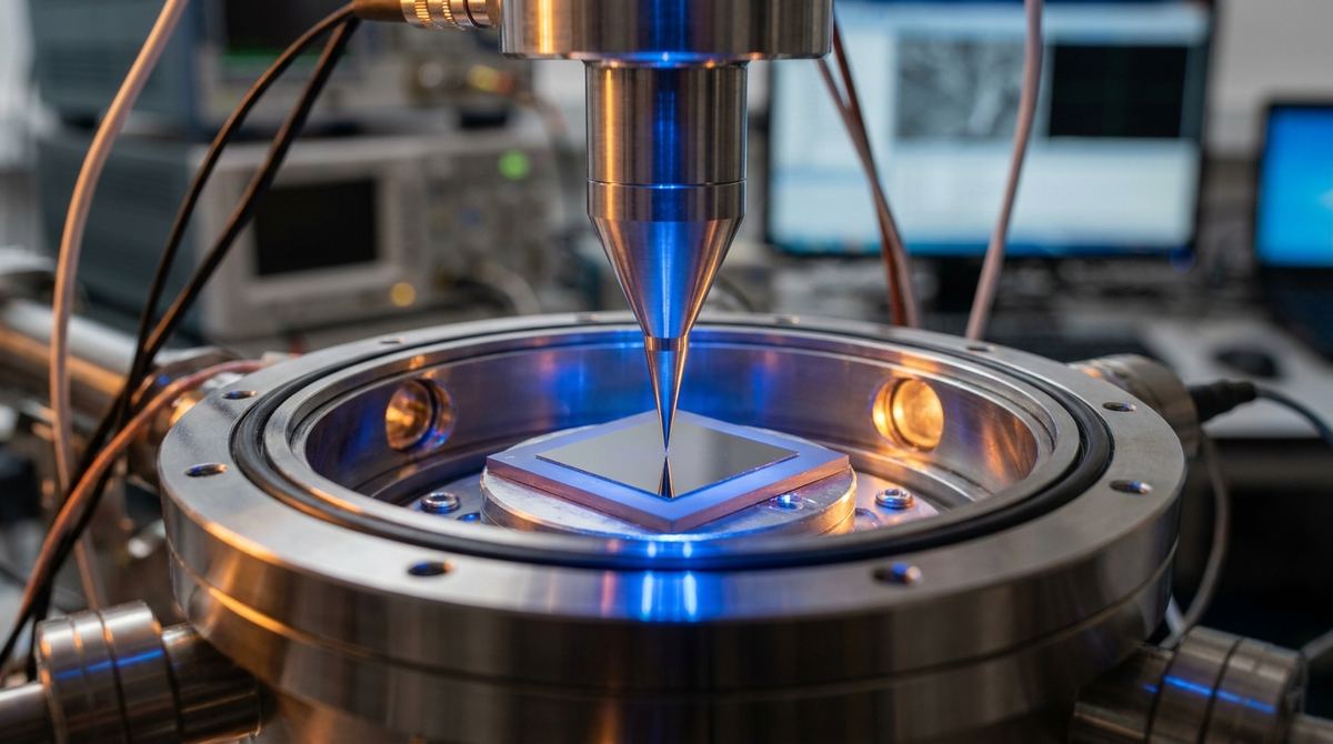
To solve this, engineers need a system that bridges the gap between the nano and the macro. This guide outlines the implementation of a dual-mode characterization platform that combines Scanning Probe Microscopy (SPM) with in situ electrical transport measurements in an ultra-high vacuum (UHV) environment.
The goal is to create a single platform where you can perform atomic-scale mapping of a graphene surface and then immediately measure the electrical resistance or critical current of that same sample. By doing this, you can directly correlate a specific structural feature (like a 5-nanometer dislocation) with a specific change in the device's total resistivity.
This requires a system that can maintain an ultra-high vacuum to prevent surface contamination, which is the primary killer of graphene mobility. By operating in a vacuum of 1x10^-11 Torr, you ensure that the graphene surface remains pristine during the transition from preparation to measurement.
Building a prototype of this scale is a significant engineering undertaking. While a small lab might start with a standard UHV chamber, achieving the performance described in recent research requires specific high-end components.
The system consists of two interconnected UHV chambers: a preparation chamber and a measurement chamber.
1. Vacuum System: You require a dual-chamber UHV setup. The base pressure must reach approximately 1x10^-11 Torr to prevent atmospheric molecules from adsorbing onto the graphene. This typically requires a combination of ion pumps and titanium sublimation pumps.
2. Cryogenic Stage: To study superconducting transitions or temperature-dependent resistivity, the measurement chamber must house a liquid-helium cryostat capable of reaching temperatures as low as 2.9 K. The system should ideally operate across a range from 2.9 K to 400 K to observe various phase transitions.
3. Dual-Mode Stage: The sample stage must be capable of both SPM (scanning) and electrical transport (4-point probe). This requires high-precision piezo-electric actuators for the SPM tip and high-stability electrical connections for the transport measurements.
4. Optical Access: To achieve rapid sample positioning, the chamber must have direct optical access. This allows for visual alignment of the tip to the sample region, which is critical for moving from a macro-scale device to a nano-scale feature within minutes.
5. Electronics: You will need custom-built, low-noise electronics for both the SPM and the transport measurements. For spectroscopy, you should aim for an energy resolution of approximately 30 microvolts to resolve superconducting gaps.
To build a functional prototype, the following materials are recommended:
- Substrate: Highly doped Silicon with a thin layer of Silicon Dioxide (SiO2) is the standard for graphene FETs.
- Graphene: High-quality CVD-grown graphene or exfoliated flakes.
- SPM Tips: For standard topography, Pt/Ir tips are standard. For advanced spectroscopy (STS), superconducting tips are required to achieve high energy resolution.
- Wiring: Gold-plated or high-purity copper wiring for electrical connections, designed for low thermal conductivity to prevent heat leak into the cryostat.
The following workflow is an engineering assumption based on the capability to move samples between chambers efficiently.
1. Sample Preparation: The graphene device is prepared in the dedicated preparation chamber. This might involve depositing metal nanowires or performing controlled chemical doping.
2. Rapid Transfer: The sample is transferred from the preparation chamber to the measurement chamber. To be practical, this transfer must be automated and rapid (target: under 10 minutes) to prevent any pressure rise that could contaminate the surface.
3. Optical Alignment: Using the integrated optical access, the operator or an automated system identifies the specific region of interest on the graphene device. The target accuracy for positioning is approximately 5 microns x 5 microns.
4. Local Mapping (SPM): The SPM tip is brought into contact with the surface. The system performs a scan to map the local topography and spectroscopic signatures of the surface.
5. Global Measurement (Transport): Without moving the sample, the system switches to electrical transport mode. You measure the resistivity, voltage-current (V-I) curves, or critical current across the device.
6. Correlation Analysis: The data from the SPM scan is overlaid with the electrical transport data to identify which local features are responsible for the macroscopic electrical behavior.
To validate your prototype, you should execute the following tests:
1. Vacuum Integrity Test: Verify the system can maintain 1x10^-11 Torr over a 24-hour period.
2. Thermal Stability Test: Measure the mechanical stability of the tip-sample junction across the temperature range of 2.9 K to 400 K. The target stability is below 1 picometer.
3. Energy Resolution Test: Using a known superconducting sample (like Lead), verify that the system can resolve the superconducting gap with a resolution of at least 30 microvolts.
4. Correlation Test: Intentionally introduce a defect (such as a local heat pulse or a chemical dopant) and observe if the resulting change in local topography/spectroscopy matches the change in the device's total resistivity.
Building this system involves several high-level technical risks:
- Vacuum Contamination: Any leak in the transfer mechanism will ruin the graphene's mobility. Mitigation: Use ultra-high vacuum-compatible seals and automated docking mechanisms.
- Thermal Drift: Moving from 400 K to 2.9 K causes significant thermal contraction. Mitigation: Use low-expansion materials (like Invar) for the stage and implement real-time optical feedback for tip positioning.
- Vibration: SPM is extremely sensitive to mechanical noise. Mitigation: The entire vacuum system should be mounted on an active vibration isolation table, and the cryostat must be decoupled from the vacuum pump.
- Electrical Noise: Measuring microvolt-scale signals in a cryostat is difficult due to thermal and electromagnetic noise. Mitigation: Use shielded, twisted-pair wiring and low-noise, high-precision current sources.
Serious about B2B integration? Test our premium Pulsed Electrical Resistive Carbon Heating turbostratic graphene in your lab. 100g sample packs available now.
Explore More
Researchers demonstrate precise control over the magnetic and structural properties of the 2D ferromagnet Fe3GeTe2 by introducing nickel atoms, a key step...

Twisted trilayer graphene allows for remote electronic control of a decoupled layer, a breakthrough in moiré physics that could enable cleaner quantum devices.

Learn a practical, polymer-free method for building a graphene FET using muscovite mica for clean transfer, assembly, and contact patterning.