
A New Era of Graphene Engineering: Pre-Designing Twist Angles on Demand
Researchers have developed a breakthrough method for growing twisted bilayer graphene with pre-designed angles, a key step toward manufacturable quantum...
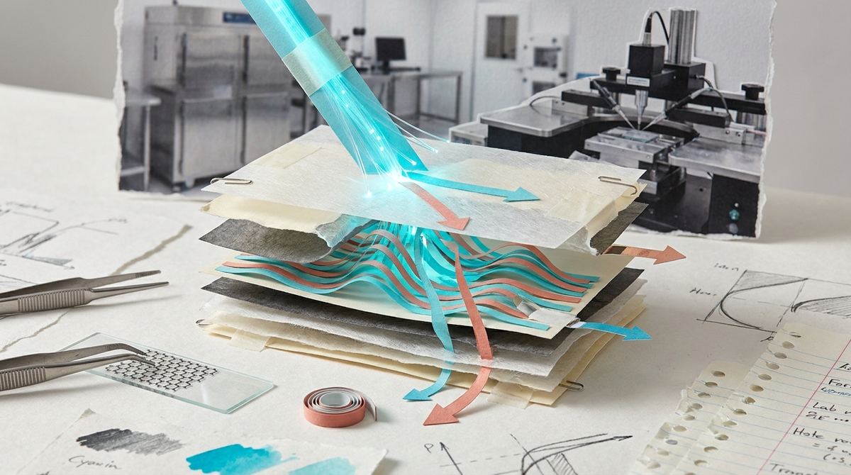
Imagine a world where the fundamental properties of a computer chip could be changed instantly, not by rewriting software or swapping out components, but simply by shining a specific color of light onto its surface. In the traditional electronics industry, we rely on permanent changes to a material to make it work, such as adding chemical impurities to increase conductivity. However, as we push toward the limits of quantum computing and ultra-fast sensing, these permanent changes often introduce unwanted defects that disrupt the delicate dance of electrons. Recent breakthroughs in the field of two-dimensional materials are changing this paradigm by allowing researchers to manipulate electrons using light, turning a static component into a dynamic, tunable system.
To understand why this research is revolutionary, one must first understand the limitations of current semiconductor technology. In standard silicon-based electronics, we achieve what is called doping, which involves intentionally introducing specific atoms into a crystal lattice to change how it conducts electricity. While effective, chemical doping is often a permanent, irreversible process. Once a material is doped, its electronic properties are essentially locked in. Furthermore, the very atoms used to dope the material can act as scattering centers, creating "bumps" in the road that impede the smooth flow of electrons.
As we move into the realm of extremely thin, two-dimensional materials, these problems become even more acute. In these ultra-thin layers, every single atom matters. Introducing chemical dopants often disrupts the pristine crystal structure of the material, leading to defects that kill the performance of the device. Moreover, many of the most interesting phenomena in physics, such as superconductivity or exotic quantum states, depend on the precise, undisturbed movement of electrons. If we cannot control the density of these electrons without destroying the material's perfection, we cannot harness the full potential of quantum materials. There is a desperate need for a method of modulation that is non-destructive, reversible, and highly precise.
The solution proposed by the research team involves using light to perform a technique known as photoinduced modulation doping. Instead of physically adding atoms to the material, researchers use photons to excite electrons into higher energy states, effectively changing how many charge carriers are available to move through the device. This is achieved within a van der Waals heterostructure, which is essentially a microscopic sandwich made of different two-dimensional materials stacked on top of one another.
By carefully choosing the materials in this stack, scientists can create a system where light hitting one layer causes electrons to move into a neighboring layer. This allows us to change the electrical properties of the conducting layer without ever touching it with a chemical. It is a way of "tuning" the material in real time. If we want more current to flow, we increase the light intensity. If we want to change how electrons interact with each other, we can change the wavelength of the light. This provides a level of in situ control—meaning control during the actual operation of the device—that was previously impossible with traditional electronic or chemical methods.
The architecture described in the study involves the precise stacking of various two-dimensional layers, often including graphene or other transition metal dichalcogenides, to form a van der Waals heterostructure. These materials are unique because they are held together by weak van der Waals forces rather than the strong covalent bonds found in bulk materials. This allows for the creation of interfaces that are atomically sharp and remarkably clean, free from the dangling bonds that usually plague semiconductor surfaces.
The mechanism of photoinduced modulation doping begins when a photon strikes the heterostructure. If the energy of the photon matches the bandgap of one of the layers in the stack, an electron is promoted from the valence band to the conduction band, creating an electron-hole pair. Because of the specific "band alignment" of the stacked layers, these newly freed electrons can be transferred from the layer that absorbed the light into a separate, adjacent layer that acts as the primary transport channel.
This transfer is the core of the "modulation" process. In a traditional device, the number of charge carriers is fixed by the manufacturing process. In this heterostructure, the number of carriers in the conducting layer becomes a function of light intensity and wavelength. This creates a high-mobility environment because the carriers in the conduction layer are spatially separated from the region where the light was absorbed. This separation prevents the electrons from colliding with the holes created by the light, which would otherwise slow them down. This separation is a critical factor in enhancing transport, as it minimizes the scattering events that typically limit electrical conductivity.
The investigation led by Collin R. Sanborn, Son T. Le, Thuc T. Mai, Maria F. Munoz, Riccardo Torsi, Angela R. Hight Walker, Curt A. Richter, Samuel W. LaGasse, Aubrey T. Hanbicki, and Adam L. Friedman revealed that this light-based tuning does more than just change conductivity; it allows for the direct manipulation of electronic correlation. Electronic correlation refers to the phenomenon where the movement of one electron is strongly influenced by the movements and positions of all other electrons in the system. In most standard conductors, these interactions are relatively weak, but in low-dimensional materials, they become dominant.
The researchers discovered that by using light to tune the carrier density, they could move the material through different electronic phases. By controlling the density of electrons, they could alter the strength of the electron-electron interactions, effectively changing the fundamental physics governing the device. This was observed through enhanced transport properties, where the movement of electrons through the heterostructure became significantly more efficient under specific photo-excitation conditions.
Crucially, the study demonstrated that this control is highly localized and dynamic. The researchers were able to demonstrate that the electronic state of the device could be modulated in situ, meaning the properties could be changed while the device was being measured. This ability to navigate the complex landscape of electronic correlations using light provides a new way to study and exploit quantum phenomena that are otherwise too delicate to observe or control with standard electrical gating.
This research is significant because it bridges the gap between fundamental quantum physics and practical device engineering. For decades, physicists have been studying "strongly correlated electron systems" to understand how collective electron behavior leads to phenomena like high-temperature superconductivity or the fractional quantum Hall effect. However, studying these effects in a lab is often difficult because the conditions required to see them are incredibly sensitive. This research provides a "knob" to turn—the ability to precisely adjust these interactions using light.
From an engineering perspective, the ability to control electronic properties via light opens a new frontier for optoelectronics. Most current optoelectronic devices, like solar cells or photodetectors, use light to generate a signal. This research suggests a future where the light does not just provide a signal but actually reconfigures the material's fundamental electrical state. This could lead to a new class of "reconfigurable" logic gates or sensors that can adapt their sensitivity or function based on the light environment they are in.
While the results are groundbreaking, it is important to distinguish these laboratory breakthroughs from commercially ready technology. The current methods used to create these van der Waals heterostructures are highly labor-intensive and often involve manual assembly of layers under specialized conditions. To be viable in mass production, these stacking techniques must be scaled up to industrial wafer sizes using automated processes.
Additionally, the efficiency of the photo-to-charge transfer process is a critical factor. In a laboratory setting, researchers can use high-powered lasers to achieve the desired effects, but an actual consumer device would need to operate efficiently using ambient light or much lower power sources. There is also the issue of thermal management; light absorption naturally generates heat, and in a nanoscale device, even a small amount of heat can disrupt the very quantum effects the researchers are trying to observe. Future studies will need to address how to achieve this modulation without significant thermal noise.
The implications for future technology are vast and span several high-tech industries. In the field of quantum computing, the ability to tune electronic correlations could lead to much more stable qubits. If we can use light to move a material into a specific quantum state and hold it there, we create a more reliable foundation for quantum information processing.
In the realm of sensing, these heterostructures could lead to ultra-sensitive light detectors. Because the electronic properties are so sensitive to photo-excitation, we could create sensors capable of detecting single photons or identifying specific wavelengths of light with unprecedented precision. This has massive implications for medical imaging, environmental monitoring, and deep-space communication.
Furthermore, the concept of light-tunable electronics could revolutionize high-speed telecommunications. As we move toward 6G and beyond, we need components that can operate at much higher frequencies than current silicon-based technology allows. The rapid response time of light-matter interaction in these 2D materials offers a potential pathway to ultra-fast, light-driven transistors and switches.
If you remember only one thing from this research, let it be this: scientists have found a way to use light to "reprogram" the electrical behavior of ultra-thin materials without damaging them, providing a precision tool to control the complex interactions between electrons.
How do van der Waals heterostructures differ from traditional semiconductors?
Traditional semiconductors like silicon are bulk materials where atoms are tightly bonded in a three-dimensional lattice. Van der Waals heterostructures are made by stacking individual layers of different 2D materials, like graphene, on top of each other. Because these layers are only held together by weak van der Waals forces, they can be combined in ways that are impossible with bulk materials, creating entirely new types of electronic environments.
Why is light better than chemical doping for these materials?
Chemical doping involves adding foreign atoms into a material to change its charge. While this works for silicon, it can introduce defects and impurities into sensitive 2D materials, which disrupts the flow of electrons. Light, however, can change the number of electrons in a material without adding any physical atoms, leaving the crystal structure pristine and perfect.
What exactly are "electronic correlations"?
Electronic correlation is a phenomenon where electrons in a material interact with each other so strongly that they cannot be treated as individual particles. Instead, they move in a coordinated way, almost like dancers in a choreographed routine. These interactions can lead to exotic states of matter, such as superconductivity, and they are very sensitive to how many electrons are present in the material.
What does "in situ control" mean in this context?
In situ means "in its original place" or "during the process." In this research, it means that the researchers can change the electrical properties of the material while the device is actively operating. This is different from a process where you would have to take the device out of a machine and chemically treat it to change its properties.
What are the potential challenges for using this in consumer electronics?
The main challenges are scalability and energy efficiency. Currently, creating these layered structures is a very delicate, slow process that is difficult to perform on a massive scale. Additionally, for these devices to work in your smartphone or laptop, the light-driven changes would need to be very efficient and wouldn't generate too much heat, which could interfere with the device's operation.
The work performed by Sanborn, Le, Mai, Munoz, Torsi, Hight Walker, Richter, LaGasse, Hanbicki, and Friedman marks a significant step forward in our ability to master the quantum world. By leveraging the unique properties of van der Waals heterostructures and the precision of light, they have demonstrated a method to tune electronic interactions and enhance charge transport without the messy consequences of traditional doping. While there is still a long road ahead to bring this technology from the laboratory to the factory floor, the ability to control matter with light opens a breathtaking new chapter in the history of electronics and quantum science.
Serious about B2B integration? Test our premium Pulsed Electrical Resistive Carbon Heating turbostratic graphene in your lab. 100g sample packs available now.
Explore More
Researchers have developed a breakthrough method for growing twisted bilayer graphene with pre-designed angles, a key step toward manufacturable quantum...

Learn how deep learning is revolutionizing the structural characterization of twisted bilayer materials, accelerating the development of next-generation...

Learn to build a prototype graphene FET biosensor for sensitive DNA detection. This guide covers materials, fabrication, and testing for point-of-care...