
A New Era of Graphene Engineering: Pre-Designing Twist Angles on Demand
Researchers have developed a breakthrough method for growing twisted bilayer graphene with pre-designed angles, a key step toward manufacturable quantum...
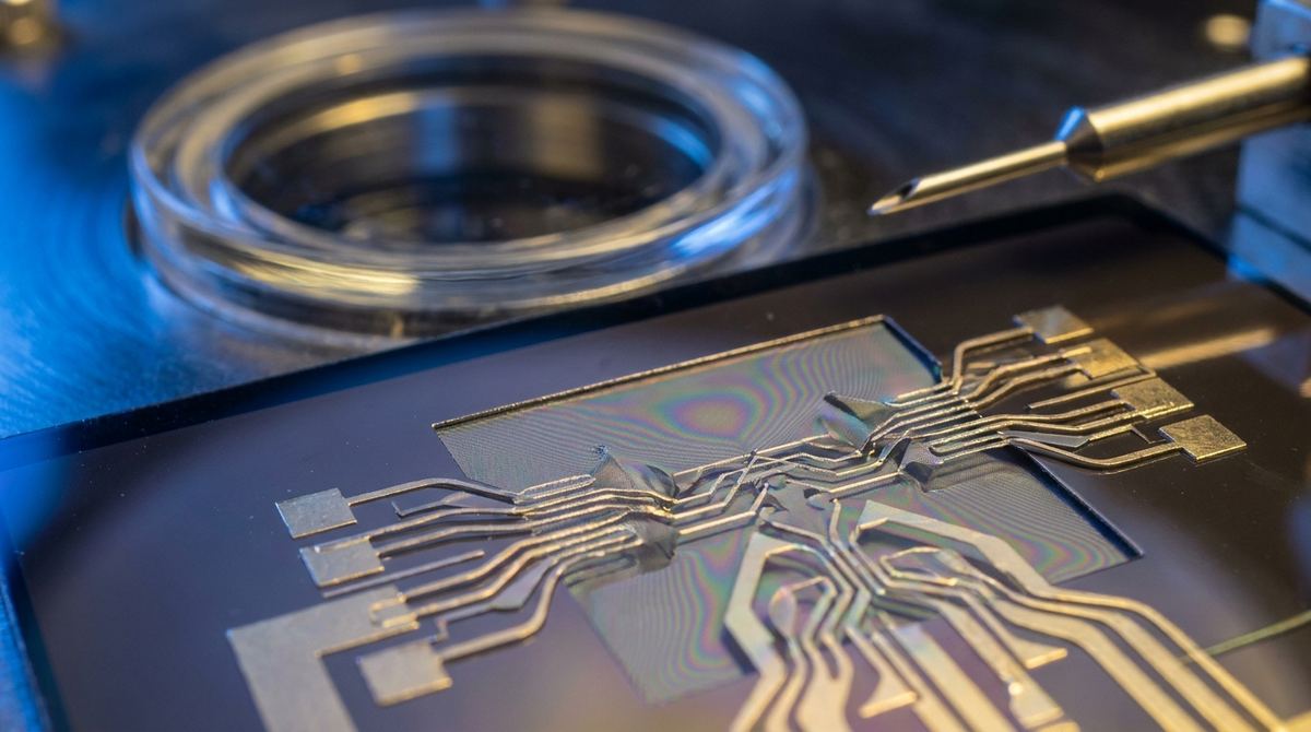
For engineers working in the semiconductor or quantum materials space, the primary hurdle in scaling twisted bilayer graphene (TBG) technology is material homogeneity. When two sheets of graphene are stacked at a specific angle, the resulting moiré pattern creates a periodic potential that can be used for highly sensitive electronic applications. However, the performance of these devices is extremely sensitive to local variations in charge density.
Even a tiny amount of unintentional doping—caused by trapped impurities, substrate roughness, or residues from the fabrication process—can create a hidden cavity within the device. These cavities act as internal potential barriers that scatter electrons and disrupt the intended electronic properties. For a startup or a research lab trying to develop high-speed transistors or quantum sensors, these local defects are often invisible to standard imaging techniques but can significantly degrade device performance.
This guide outlines a practical method for using Fabry-Pérot interference spectroscopy to non-invasively map these internal potential profiles. Instead of destroying the device to see what is inside, we use the electron waves themselves as a probe.
When electrons travel through a high-quality, ballistic graphene device, they behave like waves. If they encounter a sudden change in the local electrostatic potential (a "step" in the potential profile), a portion of the electron wave will reflect back. This creates a cavity between the source of the electrons and the potential barrier.
As you vary the gate voltage to change the carrier density, the wavelength of the electrons changes. When the wavelength satisfies a specific resonance condition relative to the size of the cavity, constructive or destructive interference occurs. This manifests as oscillations in the longitudinal resistance (Rxx) of the device.
By analyzing the frequency and pattern of these resistance oscillations, we can determine:
1. The location of the potential barrier.
2. The size of the internal cavity.
3. The magnitude of the local doping.
This technique is particularly powerful because it works in the unipolar regime, meaning we can detect these defects even when the device is intended to be uniformly doped.
To implement this characterization method, you will need a setup capable of high-precision transport measurements at cryogenic temperatures.
Materials:
1. High-quality Graphene: Ideally, CVD-grown graphene or exfoliated flakes with high carrier mobility.
2. Hexagonal Boron Nitride (hBN): Used for encapsulation to ensure ballistic transport. The hBN must be extremely clean and free of hydrocarbons.
3. Substrate: A silicon/silicon dioxide (Si/SiO2) substrate with a global back gate to allow for tuning the overall carrier density.
4. Contact Metals: Typically a combination of Chromium/Gold (Cr/Au) or Titanium/Gold (Ti/Au) for electrical connections.
Equipment:
1. Cryogenic Probe Station: The device must be cooled to extremely low temperatures, typically below 4 Kelvin (liquid Helium temperatures), to prevent thermal broadening from washing out the interference patterns.
2. Precision Source Measure Unit (SMU): To apply precise gate and drain-source voltages.
3. Magnet System: A superconducting magnet capable of applying a perpendicular magnetic field (B-field) is required to distinguish between local and global resonance modes.
4. Electron-Beam Lithography (EBL) System: For defining precise electrode patterns.
The following steps assume a standard dry-transfer stacking method, which is the industry standard for producing high-performance 2D heterostructures.
1. Substrate Preparation: Clean the Si/SiO2 substrate using standard RCA cleaning or oxygen plasma to remove organic contaminants.
2. Bottom Encapsulation: Pick up a thin flake of hBN (typically 20-50 nm thick) and place it on the substrate.
3. Graphene Layer 1: Pick up the first layer of graphene.
4. Graphene Layer 2 and Twisting: Pick up the second layer of graphene. This is the critical step. Using a high-precision rotation stage, twist the second layer relative to the first. For this specific metrology application, a large twist angle (greater than 1 degree) is recommended to avoid the complex moiré physics found at the magic-angle regime.
5. Top Encapsulation: Pick up a final layer of hBN (20-50 nm) to encapsulate the twisted bilayer structure. This protects the device from environmental degradation and ensures the electrons travel without hitting impurities.
6. Electrode Patterning: Use electron-beam lithography to define the contact areas. Perform metal evaporation (Cr/Au) to create the source and drain electrodes.
7. Final Annealing: Perform a vacuum anneal (e.g., 200-300 degrees Celsius for several hours) to remove any remaining polymer residues from the device edges.
Once the device is fabricated, follow this protocol to map the internal potential profile.
1. Resistance vs. Gate Voltage Sweep: Apply a constant drain-source voltage and sweep the back-gate voltage (V_g). Look for periodic oscillations in the longitudinal resistance (Rxx). If you see oscillations in a regime where the device should be nominally unipolar, you have identified a hidden cavity.
2. Magnetotransport Differentiation: This is the most critical step for validating your findings. Apply a perpendicular magnetic field and observe how the oscillations change.
- Global Resonances: If the oscillations are caused by the entire device size, they will show a specific, predictable dependence on the magnetic field as the cyclotron radius changes.
- Local Cavity Modes: If the oscillations are caused by a small, local defect (a hidden cavity), they will behave differently under a magnetic field. The local modes will often be more robust or show a different frequency shift compared to the global modes.
3. Simulation Comparison: Use a numerical simulation (such as a Tight-Binding model or a Landauer-Büttner formalism) to model the device. Input your observed oscillation frequencies into the simulation to extract the estimated size and depth of the potential barrier.
It is important to distinguish between the findings of the research and the practical engineering assumptions required to replicate this in a lab.
Engineering Assumptions:
- Temperature: The research implies low-temperature measurements. For a practical prototype, we assume a temperature of 4.2K (Liquid Helium) or lower is required to maintain ballistic transport.
- Twist Angle: We assume a large-angle twist. If you attempt this at the magic angle, the moiré-induced flat bands will create a massive amount of electronic complexity that will likely mask the Fabry-Pérot interference.
- Cavity Size: We assume the "hidden cavity" is significantly larger than the electron wavelength but smaller than the total device length.
Risks and Mitigation:
- Contamination: The biggest risk is the presence of "junk" interference. If your stacking process is not perfectly clean, you will see oscillations caused by polymer residue rather than the internal potential profile you are trying to map. Mitigation: Use a dedicated cleanroom and optimize the vacuum annealing process.
- Angle Precision: If the twist angle is not uniform across the flake, the interference patterns will become chaotic. Mitigation: Use high-resolution optical microscopy and AFM to verify the twist uniformity before proceeding to electrical testing.
- Thermal Smearing: If the temperature is too high, the oscillations will disappear. Mitigation: Ensure the device is in excellent thermal contact with the cryostat cold finger.
This guide is based on the methodology described in the research paper "Probing the Potential Profile of Twisted Bilayer Graphene via Fabry-Pérot Interference" (McDowell et al., 2026). The core concept of using resistance oscillations as a non-invasive probe for local defects is derived directly from the experimental findings of the authors, specifically their use of magnetotransport to distinguish between local and global resonance modes.
Serious about B2B integration? Test our premium Pulsed Electrical Resistive Carbon Heating turbostratic graphene in your lab. 100g sample packs available now.
Explore More
Researchers have developed a breakthrough method for growing twisted bilayer graphene with pre-designed angles, a key step toward manufacturable quantum...

Learn how deep learning is revolutionizing the structural characterization of twisted bilayer materials, accelerating the development of next-generation...

Learn to build a prototype graphene FET biosensor for sensitive DNA detection. This guide covers materials, fabrication, and testing for point-of-care...