
AI-Powered Characterization of Twisted Bilayer Graphene and 2D Materials
Learn how deep learning is revolutionizing the structural characterization of twisted bilayer materials, accelerating the development of next-generation...
Imagine a material whose fundamental electronic properties—whether it behaves as a metal, an insulator, or even a superconductor—could be changed not by altering its chemical composition, but simply by twisting one atomic layer relative to another. This is the revolutionary promise of "twistronics," a field centered on materials like twisted bilayer graphene. For years, the challenge has been that creating these specific twist angles was a matter of luck, a random outcome of a chaotic growth process. A recent breakthrough, however, suggests we are moving from an era of chance discovery to one of deliberate design. This new method gives scientists unprecedented control, allowing them to grow twisted graphene layers with specific, pre-designed angles, paving the way for the scalable production of materials with exotic, tunable properties.
Graphene, a single layer of carbon atoms arranged in a honeycomb lattice, is remarkable on its own. But when two layers are stacked and twisted by a very specific "magic angle" of about 1.1 degrees, the resulting electronic behavior is extraordinary. The electrons slow down dramatically, allowing their mutual interactions to dominate and giving rise to phenomena like superconductivity. The problem is that making this magic angle material, or any other specific angle for that matter, has been incredibly difficult. The dominant method for producing high-quality graphene, chemical vapor deposition (CVD), typically results in either perfectly aligned layers (known as Bernal stacking) or a random jumble of different twist angles across a sample.
Scientists could manually stack and twist small flakes of graphene, but this is a painstaking, low-yield process suitable only for fundamental laboratory research, not for building technologies. For twistronics to move from the lab to industry, a method for growing large areas of bilayer graphene with a consistent, predetermined twist angle was desperately needed. Without this control, creating reliable circuits, sensors, or quantum devices based on twisted graphene is impossible. The work by a team of researchers including Chaowu Xue, Mengzhao Sun, Zixuan Zhou, Zhuoran Yao, Li-Qun Shen, Xiao Kong, Honglong Zhao, Feng Ding, Marc Willinger, Zhongkai Liu, and Zhu-Jun Wang directly confronts this grand challenge of control and scalability in two-dimensional materials synthesis.
The core innovation behind this research is to use the atomic landscape of the growth substrate as a precise template to guide the formation of the second graphene layer. Instead of letting carbon atoms assemble randomly, the scientists meticulously controlled the chemical reaction conditions—the temperature, pressure, and flow of carbon-containing gas—to make the growth process itself angle-selective. This approach is rooted in the field of chemical kinetics, which studies the speed of chemical reactions. The team realized that by tuning the kinetics, they could create a scenario where it is far easier and faster for the second graphene layer to start growing at a specific, desired twist angle relative to the first.
Think of it like building with interlocking blocks on a textured surface. If the surface has a specific pattern of grooves, the blocks will naturally prefer to lock into place at a certain orientation. In this work, the "textured surface" is a single-crystal copper substrate with its own distinct atomic arrangement, or facets. The first layer of graphene grows in alignment with this copper. Then, by fine-tuning the growth environment, the researchers essentially change the "shape" of the incoming carbon building blocks and how they interact with the first layer. This makes them lock into a new, rotated orientation, creating the desired twist. They are not just hoping for the right angle; they are engineering the entire process to make that angle the most favorable outcome.
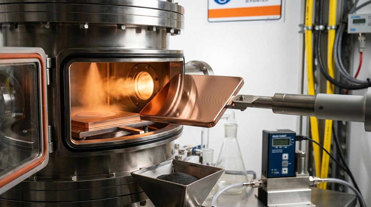
The process begins with an atomically flat, single-crystal copper foil, likely the Cu(111) facet, which has a specific triangular symmetry in its surface atom arrangement. This pristine surface is crucial because its uniformity provides the foundation for high-quality graphene growth. The substrate is heated in a vacuum chamber, and a carbon-containing gas like methane is introduced. Through the CVD process, the methane molecules break down, and carbon atoms deposit onto the hot copper surface, self-assembling into a continuous, single layer of graphene that conforms to the underlying crystal structure of the copper. This creates the first layer of the bilayer system.
The critical step is the growth of the second layer. After the first layer is complete, the growth conditions are carefully changed. This is where the "facet-dependent chemical kinetics" come into play. The researchers adjust the parameters to control the rate of nucleation—the formation of the initial tiny islands of the second graphene layer. The atomic steps and terraces of the copper substrate, along with the existing graphene layer, create a complex energy landscape. The incoming carbon species (atoms or small clusters) diffuse across this landscape. The researchers discovered a set of conditions where the energy barrier for nucleation is lowest at a specific rotational angle.
This means that the second-layer graphene islands are kinetically "trapped" into forming with a pre-designed twist. It is the fastest reaction pathway available under those specific conditions. As more carbon is supplied, these precisely-oriented islands grow and merge, eventually forming a continuous second graphene layer with a uniform, non-random twist angle across the entire sample. This method transforms the growth process from a thermodynamically-driven one (which would favor zero-twist stacking) to a kinetically-governed one, where the speed of formation dictates the final structure.
The team successfully demonstrated that this kinetically-governed approach works. Using advanced imaging techniques like transmission electron microscopy, they were able to visualize the resulting moiré patterns—the large-scale interference pattern created by the two misaligned graphene lattices. These patterns serve as a direct fingerprint of the twist angle, and their uniformity confirmed that the researchers had produced large domains of bilayer graphene with a single, specific rotation. They showed that by systematically varying the growth parameters, such as the partial pressure of the methane precursor and the temperature, they could reliably select different target angles.
Crucially, their experimental results were supported by a robust theoretical model. This model explains how the interaction between the carbon precursors, the first graphene layer, and the underlying copper facet dictates the nucleation kinetics. It provides a predictive framework, allowing them to understand which conditions will lead to which angles. This elevates the work from a clever recipe to a true scientific principle. They established a clear cause-and-effect relationship between the controllable process parameters and the final atomic structure of the material. This is a foundational achievement, providing a roadmap for rationally designing twisted 2D materials.
This breakthrough represents a paradigm shift in the synthesis of 2D materials. It marks a transition from discovering materials with interesting properties to designing and manufacturing them with those properties built-in from the start. For the field of twistronics, this is a game-changer. The ability to reliably produce wafer-scale twisted bilayer graphene with a specific angle is the enabling technology required for creating functional electronic devices. This moves the material from a laboratory curiosity to a viable candidate for next-generation technologies, representing a significant advance in graphene manufacturing techniques.
By providing a reliable source of high-quality, angle-specific bilayer graphene, this research could dramatically accelerate progress in fundamental physics and applied technology. Scientists will no longer have to hunt for tiny, randomly-oriented flakes to study exotic quantum phenomena. Instead, they can order or produce a wafer with the exact twist angle they need to test a hypothesis. This could unlock the full potential of graphene electronics, enabling the development of novel devices like ultra-low-power transistors, highly sensitive photodetectors, and components for quantum computers. The ability to tune electronic properties through geometry is a powerful new tool in the materials scientist's arsenal.
While this research is a monumental step forward, it is important to recognize its current limitations. The work described is a proof-of-concept, likely demonstrated on a laboratory scale. Translating this precise, kinetically-controlled process to an industrial scale presents significant engineering hurdles. The growth process is likely extremely sensitive to minute fluctuations in temperature, pressure, and gas purity, which are much harder to control in a large-scale production environment. Achieving perfect uniformity over entire wafers will require the development of highly sophisticated graphene production machinery with unprecedented process control.
Furthermore, the paper likely demonstrates control over a specific set of angles determined by the substrate symmetry and the chemical system used. It is not yet clear if this method can be adapted to produce any arbitrary twist angle on demand. The long-range quality and electronic performance of the grown material also need extensive characterization. While the twist angle may be uniform, the material must also have a low density of defects and impurities to be useful for high-performance electronics. Rigorous testing of the material's transport properties, such as its conductivity and superconducting behavior, is the essential next step to validate its technological potential.
Assuming the challenges of scalability and quality control can be overcome, the potential applications are vast and transformative. In quantum computing, the unique electronic states in magic-angle graphene could be used to create stable and reproducible qubits, the fundamental building blocks of quantum processors. In the realm of sensors, devices made from twisted bilayer graphene could be exquisitely sensitive to electric fields, magnetic fields, or the presence of specific molecules, as these external stimuli would strongly affect its finely balanced electronic state.
For conventional electronics, this technology could lead to entirely new types of transistors that can be reconfigured on the fly, or devices that combine logic and memory functions. In photonics, the material could be used to create efficient detectors and modulators for terahertz radiation, a portion of the electromagnetic spectrum that is difficult to work with but holds promise for high-speed communications and medical imaging. This control over the material's fundamental properties opens up design possibilities that were previously confined to theory.
If you take away just one idea from this breakthrough, it should be this: scientists have learned how to use the atomic structure of a metal surface as a programmable template to build twisted graphene layers with specific, engineered angles. By precisely controlling the speed of the chemical reactions during growth, they can now dictate the final structure of the material, turning what was once a game of chance into a deterministic manufacturing process and opening the door to custom-designed quantum materials.
What is twisted bilayer graphene?
Twisted bilayer graphene is a material made of two sheets of graphene stacked on top of each other with a slight rotational misalignment. This rotation creates a large-scale interference pattern called a moiré superlattice, which fundamentally changes the material's electronic properties compared to a single graphene sheet or two perfectly aligned sheets. This structure is distinct from the more randomly oriented layers found in materials like turbostratic graphene flakes, which lack a consistent, long-range twist angle.
Why is the "magic angle" in twisted graphene so special?
The "magic angle," approximately 1.1 degrees, is special because at this precise twist, the electronic bands of the graphene flatten out. This means electrons move very slowly and their interactions with each other become much stronger than their individual kinetic energy. This strong correlation leads to the emergence of exotic quantum phenomena, including unconventional superconductivity and correlated insulating states, which are of immense interest to physicists.
What does "facet-dependent" mean in this context?
"Facet-dependent" means the growth process is critically influenced by the specific crystal face of the substrate being used. A crystal like copper has different atomic arrangements on its different surfaces, or facets, such as the (111) or (100) face. The researchers leveraged the unique atomic geometry of a specific facet to act as a template, guiding the orientation of the second graphene layer during growth.
How is this new growth method different from previous ones?
Previous methods for making twisted bilayer graphene either involved the manual and painstaking process of stacking and twisting tiny exfoliated flakes or relied on CVD growth that produced a random distribution of twist angles. This new method is fundamentally different because it is deterministic. It uses kinetic control to actively guide the growth process toward a single, pre-selected twist angle over a large area, representing a shift from discovery to design.
Is this technology ready for commercial products?
No, this technology is still in the early stages of research and development. While it represents a critical scientific breakthrough, significant engineering work is required to scale up the process, ensure perfect quality and reproducibility, and integrate the material into functional devices. As with any advanced material, the path to commercialization will involve overcoming these challenges and understanding the economic viability, which is tracked in graphene market research.
The ability to grow twisted graphene layers with pre-designed angles by governing facet-dependent chemical kinetics is more than just an incremental improvement; it is a foundational leap forward in materials science. It provides a powerful new tool for engineering the quantum properties of matter at the atomic scale. By understanding and controlling the intricate dance of atoms on a crystal surface, the research team has laid the groundwork for a future where materials with exotic properties like superconductivity can be manufactured on demand. This work transforms twisted bilayer graphene from a fascinating object of study into a credible platform for building the next generation of quantum and electronic technologies.
Serious about B2B integration? Test our premium Pulsed Electrical Resistive Carbon Heating turbostratic graphene in your lab. 100g sample packs available now.
Explore More
Learn how deep learning is revolutionizing the structural characterization of twisted bilayer materials, accelerating the development of next-generation...

Learn to build a prototype graphene FET biosensor for sensitive DNA detection. This guide covers materials, fabrication, and testing for point-of-care...

Discover how hopping-mediated charge transport explains graphene's electrical behavior beyond the ideal ballistic regime, a key insight for creating...