
AI-Powered Characterization of Twisted Bilayer Graphene and 2D Materials
Learn how deep learning is revolutionizing the structural characterization of twisted bilayer materials, accelerating the development of next-generation...
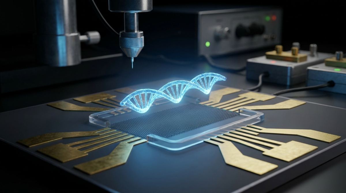
The field of biomedical diagnostics is on the cusp of a revolution, driven by nanomaterials that can detect diseases at the molecular level with unprecedented speed and accuracy. Among these materials, graphene stands out. Its unique electronic properties make it an ideal candidate for the active component in next-generation biosensors.
A 2026 review by Sikhamani, Panda, and Raut titled "Two-dimensional graphene and transition metal dichalcogenide field effect transistor biosensors" highlights the immense potential of graphene-based field-effect transistors (G-FETs) for medical sensing. This guide translates the principles from that research into a practical framework for an engineering team, small lab, or startup looking to build a functional prototype. We will focus on one specific, high-impact application: a liquid-gated G-FET biosensor designed for the label-free detection of specific DNA sequences.
The goal is to fabricate a G-FET biosensor. At its core, this device operates like a standard transistor, but with a critical modification: the "gate" that controls the flow of electricity is influenced by a biological environment.
The device consists of a single layer of graphene transferred onto a silicon dioxide (SiO2) on silicon (Si) wafer. This graphene layer acts as the semiconductor channel. Two metal contacts, the source and drain, are patterned on top of the graphene.
In our design, we will use a liquid-gate configuration. Instead of a solid top-gate material, the graphene channel will be exposed to a liquid sample contained within a small well. A reference electrode (like Ag/AgCl) is submerged in this liquid, applying a gate voltage through the solution.
The principle of detection is elegantly simple. The graphene surface is "functionalized" with single-stranded DNA probes that are complementary to the target DNA sequence you want to detect. When the target DNA is present in the sample, it hybridizes (binds) with the probes. DNA molecules carry a negative charge. This binding event introduces a significant number of negative charges near the graphene surface, altering the local electric field. This change in the electric field acts like a change in the gate voltage, modulating the conductivity of the graphene channel. By measuring the change in current flowing from source to drain, you can detect the presence and even the concentration of the target DNA.
The 2026 review by Sikhamani et al. provides the scientific foundation for this project. The authors emphasize several key points that justify our design choices.
First, the selection of graphene is paramount. The paper notes graphene's "remarkable carrier mobility and ambipolar transport," which are the sources of its high sensitivity. Electrons and holes move through graphene with very little resistance, meaning even a tiny disturbance in the local electric field from a few bound DNA molecules can cause a measurable change in the channel's conductivity. This is the property that enables the potential for single-molecule detection, a future direction mentioned in the paper.
Second, the choice of a Field-Effect Transistor (FET) architecture is a strategic one. The review methodically examines various FET configurations, including back-gate, liquid-gate, and dual-gate structures. For biomedical applications where the sample is inherently liquid, the liquid-gated FET is a natural fit. It allows for direct interaction between the analyte (the target DNA in the sample) and the sensing surface (the graphene channel). This configuration is essential for real-time detection, a key feature for point-of-care diagnostics.
The paper also discusses the challenges, which we must address in our design and testing. These include material uniformity, device-to-device variability, and environmental stability. Our fabrication and testing protocols are designed to mitigate these issues where possible and to characterize their impact on performance.
This list assumes access to a basic microfabrication facility. For startups or smaller labs, some of these processes, like photolithography and metal deposition, can often be outsourced to university cleanrooms or commercial services.
Materials:
Substrate: 4-inch p-doped Silicon wafer with a 300 nm thermally grown SiO2 layer.
Graphene: Monolayer graphene grown via Chemical Vapor Deposition (CVD) on a copper foil. High-quality CVD graphene is crucial for consistent electronic performance. For initial proof-of-concept work with lower performance expectations, a solution of turbostratic graphene flakes could be spin-coated, though this introduces significant variability.
Metal Contacts: Chromium (Cr, 5 nm thickness) for adhesion and Gold (Au, 50 nm thickness) for the conductive layer.
Chemicals: Acetone, Isopropyl Alcohol (IPA), deionized (DI) water for cleaning. Photoresist (e.g., AZ 5214-E) and developer for lithography.
Biochemicals:
Linker Molecule: 1-pyrenebutanoic acid succinimidyl ester (PBASE). This molecule has a pyrene group that attaches non-covalently to the graphene lattice via pi-pi stacking, and an NHS ester group to bind with the DNA probes.
Probe DNA: A custom-synthesized single-stranded DNA (ssDNA) sequence with an amine group (NH2) at one end. This sequence should be complementary to your target.
Target DNA: The complementary ssDNA sequence you wish to detect.
Buffer Solution: Phosphate-buffered saline (PBS) at a specific pH (e.g., 7.4) is a common choice for maintaining biological stability.
Equipment:
Spin coater
Hot plate
Mask aligner for photolithography
Thermal or e-beam evaporator for metal deposition
Reactive Ion Etcher (RIE) with oxygen plasma capability
Tube furnace for annealing
Probe station connected to a semiconductor parameter analyzer (e.g., Keithley 4200-SCS)
Reference electrode (Ag/AgCl)
Fabricating a G-FET is a multi-step process requiring precision. The exact parameters (spin speeds, exposure times, etc.) will depend on your specific equipment and materials. The following steps provide a general workflow.
1. Substrate Cleaning: Thoroughly clean the SiO2/Si wafer by sonicating it sequentially in acetone, IPA, and DI water for 10 minutes each. Dry with a nitrogen gun.
2. Graphene Transfer: Transfer the CVD graphene from its copper foil to the SiO2/Si substrate. The wet transfer method using a PMMA support layer is standard. This is a delicate process and a primary source of defects.
3. Electrode Patterning: Spin-coat the photoresist onto the graphene/SiO2/Si substrate. Use a photomask designed with your source-drain electrode geometry to expose the resist with UV light. Develop the resist to create openings where the metal will be deposited.
4. Metal Deposition: Place the substrate in a thermal evaporator. Deposit 5 nm of Cr followed by 50 nm of Au. The chromium layer is essential for the gold to adhere properly to the SiO2 surface.
5. Lift-off: Submerge the wafer in an acetone bath. The acetone will dissolve the remaining photoresist, lifting off the metal on top of it and leaving only the desired metal electrodes in contact with the graphene.
6. Graphene Channel Definition: To isolate individual devices and prevent crosstalk, the graphene between devices must be removed. Use another photolithography step to protect the active channel area with photoresist. Then, use a low-power oxygen plasma in an RIE system to etch away the unprotected graphene.
7. Annealing: Anneal the device in a tube furnace under an Argon/Hydrogen atmosphere. A cautious starting point, based on common literature, would be 300°C for 2 hours. This step helps remove polymer residues from the fabrication process and improves the electrical contact between the metal and graphene.
8. Encapsulation: Define the liquid sensing well. Use a thick, biocompatible photoresist like SU-8. Pattern it to create an opening that exposes only the graphene channel and a small portion of the source-drain electrodes, while passivating the rest of the device.
This is where the device becomes a biosensor. All steps should be performed carefully in a clean environment to avoid contamination.
1. Baseline Characterization: Before adding any biological components, characterize the electrical properties of the bare G-FET. Place a droplet of PBS buffer in the sensing well, insert the Ag/AgCl reference electrode, and connect the source and drain to the semiconductor parameter analyzer. Sweep the liquid-gate voltage (Vlg) from -1V to +1V and measure the source-drain current (Ids) at a constant low bias (e.g., Vds = 50 mV). This will give you the transfer curve (Ids vs. Vlg) for the pristine device. The voltage at which the current is at a minimum is the Dirac point (V_Dirac).
2. Surface Functionalization: Prepare a solution of PBASE in a solvent like dimethylformamide (DMF). The source literature does not specify a concentration, so a cautious starting point is 1-2 mM. Incubate the device with this solution for 1-2 hours at room temperature, then rinse thoroughly with DMF and DI water to remove any unbound molecules.
3. Probe DNA Immobilization: Prepare a solution of your amine-terminated ssDNA probes in PBS buffer. A typical starting concentration is 1 µM. Incubate the functionalized device with the probe solution for another 1-2 hours, allowing the amine groups on the DNA to form covalent bonds with the NHS ester groups on the PBASE linkers. Rinse thoroughly with PBS buffer.
4. Target DNA Detection: After immobilizing the probes, measure the transfer curve again in fresh PBS buffer. This new curve will be your baseline for detection. Now, introduce your sample containing the target DNA sequence into the sensing well. Allow it to incubate for a period, for example, 30 minutes, to allow for hybridization.
5. Final Measurement: After incubation, rinse gently with PBS to remove unbound target DNA. Measure the final transfer curve. Successful hybridization of the negatively charged target DNA will cause a positive shift in the Dirac point. The magnitude of this shift is proportional to the concentration of the bound target DNA.
A rigorous test plan is essential to validate your sensor's performance.
Specificity Test: This is crucial. Run a control experiment using a non-complementary DNA sequence. If your sensor is specific, you should see little to no shift in the Dirac point after incubation with this non-target sequence.
Sensitivity Test (Limit of Detection): Prepare samples with serially diluted concentrations of the target DNA (e.g., from 1 µM down to 1 fM). Measure the Dirac point shift for each concentration. Plot the shift versus concentration to generate a calibration curve. The lowest concentration that produces a statistically significant signal above the noise floor is your limit of detection (LOD).
Real-Time Monitoring: The Sikhamani et al. review highlights the capacity for real-time detection. You can test this by fixing the gate voltage at the point of maximum slope on your transfer curve (where the sensor is most sensitive) and monitoring the current (Ids) over time as you inject the target DNA into the well. You should observe a rapid change in current as hybridization occurs.
As the source paper notes, moving from a lab prototype to a reliable product involves overcoming significant hurdles.
Material Quality and Uniformity: The performance of your G-FET is entirely dependent on the quality of your graphene. Defects, wrinkles, and contamination from the transfer process can create massive device-to-device variability. This is a primary challenge in scalable graphene production.
Stability and Reproducibility: The non-covalent PBASE functionalization is gentle on the graphene but may not be as stable over time as covalent methods. Furthermore, achieving reproducible surface chemistry across many devices is difficult.
Biofouling: In a real-world sample like blood or saliva, countless other proteins and molecules are present. These can non-specifically bind to the graphene surface, creating false signals. Developing anti-fouling surface coatings is an active area of research in the graphene biomedical field.
Integration with Electronics: For a true point-of-care device, the sensor must be integrated with readout electronics. The challenges of CMOS compatibility and signal processing are non-trivial aspects of developing commercial graphene electronics.
This guide provides a detailed roadmap for prototyping a G-FET biosensor based on the principles outlined in leading-edge research. While the path is challenging and requires a multidisciplinary skill set, the potential reward is immense: a highly sensitive, real-time diagnostic tool that could change the face of modern medicine.
Serious about B2B integration? Test our premium Pulsed Electrical Resistive Carbon Heating turbostratic graphene in your lab. 100g sample packs available now.
Explore More
Learn how deep learning is revolutionizing the structural characterization of twisted bilayer materials, accelerating the development of next-generation...

Discover how hopping-mediated charge transport explains graphene's electrical behavior beyond the ideal ballistic regime, a key insight for creating...

A practical guide to fabricating a flexible graphene fiber sensor for the simultaneous detection of nitric oxide and H2O2, key cancer biomarkers.