
Unlocking Quasicrystal Physics in 30-Degree Twisted Bilayer Graphene
Research on 30° quasi-periodic twisted bilayer graphene reveals a unique, fractal-like energy structure under magnetic fields, paving the way for novel...
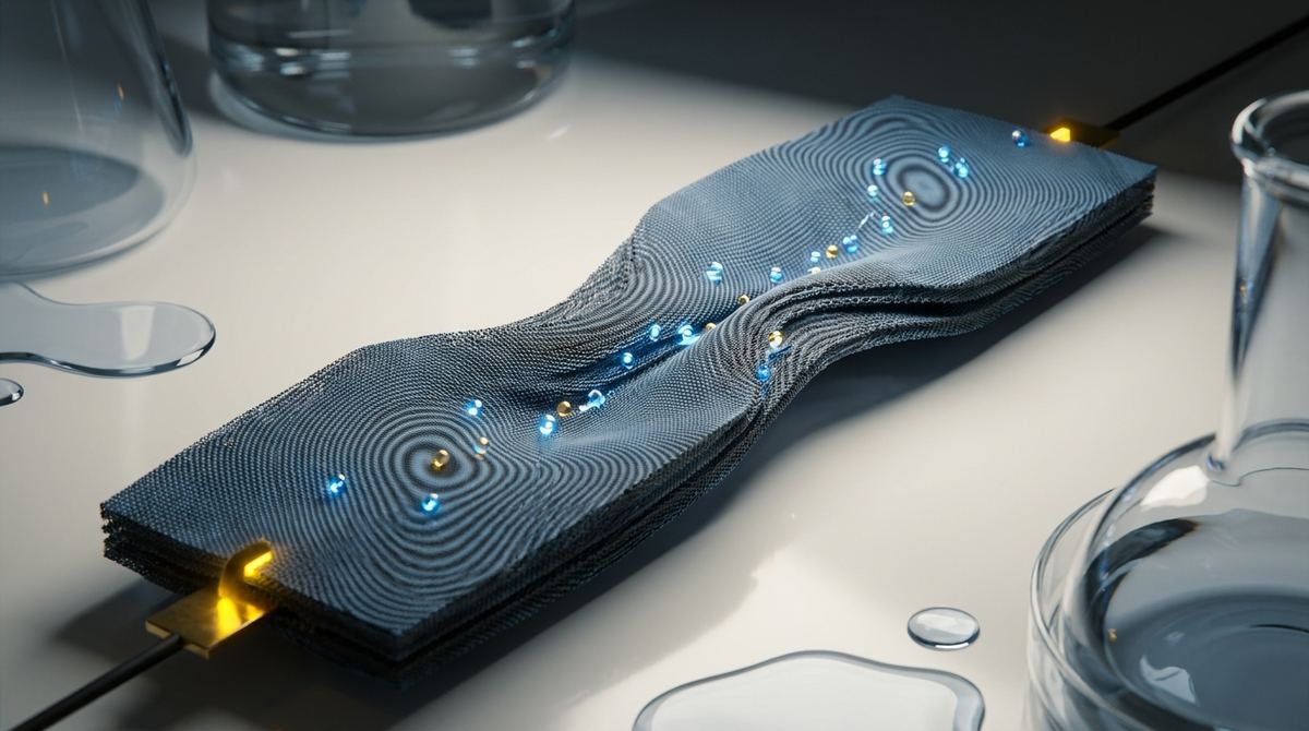
Imagine trying to design a high-speed railway system where the tracks are not straight, but are made of a landscape of hills and valleys that change every few nanometers. To build such a system, you would need a map that shows not just the general direction of the tracks, but the exact topography of every single hill and valley at an atomic scale. This is precisely the challenge facing scientists working with twisted graphene. By slightly rotating layers of carbon atoms, researchers create a new landscape known as a moiré superlattice, which fundamentally changes how electrons move. In a groundbreaking study, Sean M. Walker, Patrick Sarsfield, Isaac Soltero, Xue-Ying LiYang, Laurent Molino, Ryan Plumadore, Kenji Watanabe, Takashi Taniguchi, Vladimir Falko, and Adina Luican-Mayer have begun to map these microscopic landscapes. Their work focuses on the locally resolved electronic textures of reconstruction domains in marginally twisted monolayer-bilayer graphene, providing a much-needed look at the intricate patterns electrons form within these complex atomic environments.
The field of two-dimensional materials has long been dominated by the search for the perfect graphene structure. For years, the scientific community has understood that graphene is an exceptional conductor of electricity. However, a new frontier has emerged called twistronics, which suggests that by simply rotating one layer of graphene relative to another, we can create entirely new states of matter that do not exist in a single sheet. The problem is that these twisted structures are rarely uniform. When you twist two layers of graphene, the atoms do not just sit in a perfectly smooth, rotated pattern. Instead, the atoms undergo a process called reconstruction.
In these reconstruction domains, the atoms shift their positions to find the lowest energy state, creating a patchwork of different stacking orders. This creates a massive headache for engineers and physicists alike. If the material is a patchwork of different domains, how do we know how an electron will behave as it travels through the sample? Traditional measurements often only provide an average view of the entire material, similar to measuring the average temperature of a city rather than knowing the temperature of a specific street corner. To build functional quantum devices, we cannot rely on averages. We need to know the local electronic textures—the specific ways in which charge density and energy levels fluctuate within a single, tiny domain. Without this local resolution, we are essentially trying to engineer a precision machine while wearing a blindfold.
To understand this research, you must first understand the concept of a moiré pattern. Think of looking through two window screens, one slightly offset from the other. You will see a new, much larger pattern of light and dark spots emerging from the overlapping mesh. This is a moiré pattern. In graphene, the "mesh" is the atomic lattice of carbon atoms. When you twist two layers, you create a moiré superlattice that is much larger than the individual atoms.
The key idea explored by this research is that these moiré patterns are not just visual illusions; they create a new physical environment for electrons. Within this environment, the atoms actually rearrange themselves into clusters or domains to minimize the energy of the system. These clusters are the reconstruction domains. Instead of seeing a continuous, smooth twist, the electrons see a series of islands. Each island has its own unique electronic personality, or texture. The researchers aimed to go beyond just seeing the islands and started mapping the actual electronic "weather" inside those islands. By resolving these textures locally, they can understand how the physics of the material changes from one nanometer to the next.
The system used in this study is a highly sophisticated stack of ultra-thin materials. Specifically, the researchers used a monolayer of graphene placed directly on top of a bilayer of graphene. This monolayer-bilayer setup is particularly interesting because the interaction between the single layer and the double layer creates a unique set of physical rules for the electrons. When the twist angle between these layers is very small—what we call a marginal twist—the moiré superlattice becomes extremely large and the atomic movements become very significant.
The physics of the system is driven by the competition between the natural hexagonal lattice of the carbon atoms and the energetic desire for the atoms to settle into a more stable, stacked configuration. This competition forces the atoms to shift, creating the reconstruction domains mentioned earlier. To observe these effects, the researchers must work in extremely controlled environments, often using specialized microscopy techniques that can probe the electronic density of states at a nearly atomic scale. As the electrons move through the system, they are influenced by the local atomic arrangement. If an atom has shifted slightly to accommodate the twist, it changes the local electrical potential. This change in potential acts like a tiny hill or valley for the electron, creating the electronic textures that the team sought to resolve.
The research provides a detailed look at the electronic textures within these reconstruction domains. The findings reveal that the electronic properties are not distributed uniformly even within a single domain. Instead, the researchers observed that the local density of states—a measure of how many electronic states are available at a certain energy level—varies significantly across the landscape of the moiré superlattice.
By using high-resolution local probes, the team was able to see how the electronic textures respond to the structural boundaries of the reconstruction domains. They found that the edges of these domains, where one stacking order meets another, create unique electronic environments that are distinct from the center of the domains. This means that the electronic properties of a twisted graphene device are defined not just by the twist angle, but by the specific pattern of domains and the textures within them. This discovery highlights that the "magic" of twistronics is not just in the rotation itself, but in the complex, heterogeneous landscape that the rotation creates at the atomic scale. This mapping provides the first high-resolution blueprint of how charge is distributed in these marginal twist systems.
This research is fundamental for the development of "designer" quantum materials. For decades, materials science was about finding useful materials in nature. With the discovery of moiré physics, materials science has shifted toward creating new materials through precise geometric manipulation. However, to move from curiosity-driven science to engineering-driven technology, we must be able to predict exactly how these patterns will behave.
By understanding the local electronic textures, scientists can now predict how to tune the properties of graphene. If we know that a certain domain structure creates a specific electronic texture, we can theoretically design a device that uses that texture to perform a specific task, such as carrying a current without any resistance or acting as a sensitive sensor. This moves the field from a stage of accidental discovery to one of intentional design. It provides the necessary data to bridge the gap between abstract mathematical models of moiré physics and the actual, messy reality of physical atomic lattices.
While this research is a significant leap forward, it is important to recognize the current limitations. The studies were conducted on highly specialized, ultra-clean samples created in a laboratory setting. These are typically van der Waals heterostructures, which are incredibly fragile and difficult to produce at scale. The current methods of observing these textures require extremely sensitive equipment and often require the samples to be kept at extremely low temperatures to prevent thermal noise from obscuring the delicate electronic signals.
Furthermore, translating these findings from a microscopic, single-domain observation to a macroscopic, industrial-scale application is a monumental challenge. We do not yet know how to manufacture large-area twisted graphene that maintains such precise domain textures across an entire wafer. Future research must focus on whether these electronic textures can be controlled and reproduced in larger, more robust materials, such as those produced through chemical vapor deposition (CVD), which is the standard for industrial semiconductor manufacturing.
The implications of mastering electronic textures in twisted graphene are vast and span multiple high-tech industries. One of the most promising areas is quantum computing. The unique electronic states found in moiré superlattices could be used to create topological qubits, which are much more stable and resistant to error than current technologies. If we can control the local texture, we can control the quantum information.
In the realm of sensing, these materials could lead to the next generation of ultra-sensitive detectors. Because the electronic texture is so sensitive to the local atomic environment, even a single molecule landing on the surface could cause a measurable change in the electronic landscape. This would allow for sensors capable of detecting trace amounts of chemicals or biological markers with unprecedented precision. Additionally, the ability to tune the electronic properties via the twist angle opens doors for advanced optoelectronics, such as new types of light-emitting diodes or highly efficient solar cells that can capture a broader spectrum of light by exploiting the unique energy levels in the moiré superlattice.
If you remember only one thing from this research, let it be this: the physics of the future will not be found in uniform materials, but in the precise, intentional engineering of atomic textures and patterns.
What is the difference between regular graphene and twisted graphene? Regular graphene is a single or multiple layer of carbon atoms arranged in a perfect, uniform hexagonal lattice. Twisted graphene is created by placing layers of graphene on top of each other and rotating them by a specific angle. This rotation creates a new, larger periodic pattern called a moiré superlattice, which changes the material's fundamental electronic properties.
Why do the atoms move when you twist the layers? Atoms naturally want to be in the most stable, lowest-energy configuration. When you twist the layers, the atoms in the top layer and the bottom layer are no longer perfectly aligned. To minimize the energy caused by this misalignment, the atoms shift their positions, creating regions of different stacking orders known as reconstruction domains.
What is a moiré superlattice? A moiré superlattice is a large-scale pattern that emerges when two similar periodic structures, like two layers of carbon atoms, are overlaid with a slight misalignment. This pattern has a much larger periodicity than the original atomic lattice, creating a new playground where electrons experience a completely different set of physical rules.
Why can't we use these materials in our smartphones today? While the potential is enormous, these materials are currently very difficult and expensive to manufacture at scale. Most current research requires extremely small, highly controlled samples that must be kept at very low temperatures. Moving from a laboratory sample to a mass-produced microchip requires breakthroughs in manufacturing and stability.
What are electronic textures? Electronic textures refer to the local variations in the density and energy of electrons within a material. Instead of electrons flowing through a material like water through a smooth pipe, they move through a landscape of hills and valleys. These "textures" are the physical manifestation of how the underlying atomic arrangement influences the behavior of the electrons.
The research conducted by Walker, Sarsfield, and their colleagues marks a pivotal moment in the study of two-dimensional materials. By moving beyond the average properties of twisted graphene and zooming in on the local electronic textures of reconstruction domains, they have provided the roadmap necessary for the next era of quantum engineering. While the path from laboratory discovery to industrial application remains filled with challenges, the ability to map the atomic landscape of graphene is a profound step toward a future where we can design matter with atomic precision.
Serious about B2B integration? Test our premium Pulsed Electrical Resistive Carbon Heating turbostratic graphene in your lab. 100g sample packs available now.
Explore More
Research on 30° quasi-periodic twisted bilayer graphene reveals a unique, fractal-like energy structure under magnetic fields, paving the way for novel...

Researchers discover naturally formed graphene sheets and carbon ovals in stingless bee hives, creating a novel emergent material with powerful blue light...

Discover how rippled graphene pores act as fluidic memristors, enabling advanced synaptic functionalities for the next generation of neuromorphic computing.