
Rippled Graphene Pores for Neuromorphic Fluidic Memristive Devices
Discover how rippled graphene pores act as fluidic memristors, enabling advanced synaptic functionalities for the next generation of neuromorphic computing.
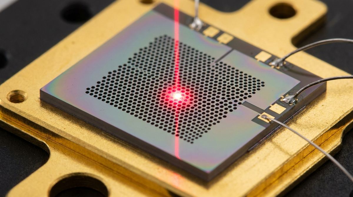
In the field of nanophotonics, mimicking the behavior of electrons in graphene has become a powerful way to control light. While electronic graphene relies on the movement of electrons in a carbon lattice, photonic graphene uses the geometry of a honeycomb lattice of air holes in a dielectric material to control photons.
Recent research by Wang et al. (2026) has introduced a breakthrough method for engineering these photonic structures. Traditionally, creating flat bands—regions where light moves very slowly and interacts strongly with matter—required extremely complex and perfect fabrication. The new research demonstrates that by applying a simple density-wave perturbation (a periodic displacement of the lattice holes), we can engineer these flat bands and even create topological interface states.
For engineers and startups, this is significant. It provides a predictable, fabrication-friendly way to create localized light modes that are topologically protected. This is the foundation for a new class of sensors and nonlinear optical devices that are much more robust than traditional resonators.
The research focuses on a single-layer honeycomb photonic crystal slab. In a perfect honeycomb lattice, light behaves according to the symmetry of the holes. However, the authors suggest a method to "program" the light by slightly shifting the position of each hole.
Instead of the holes being placed at perfect coordinates, each hole is displaced by a small amount following a periodic function, such as a sine or cosine wave. This is the density-wave perturbation. By controlling the frequency and amplitude of this displacement, you can manipulate the band structure of the photonic crystal.
Specifically, this modulation allows you to create a Dirac mass term. In physics terms, this "mass" determines how the light waves propagate. By tuning this mass, you can flip the topological phase of the material. When you place two regions with opposite topological phases next to each other, a Jackiw-Rebbi interface state is formed. This state is a localized mode of light that exists strictly at the boundary between the two regions.
The most practical application for a small lab or startup is a Topological Interface Sensor.
In a standard resonator-based sensor, the light is sensitive to the environment, but it is also highly sensitive to fabrication errors and temperature shifts. In a topological interface sensor, the light is trapped at the interface between two domains of different topological mass. Because this state is topologically protected, it is much more robust against minor manufacturing imperfections.
To use this for sensing, you would introduce a target analyte (such as a gas or a liquid) into the holes at the interface. The presence of the analyte changes the local refractive index, which shifts the frequency of the localized interface state. Because the light is highly concentrated at that specific junction, the sensitivity to local refractive index changes is significantly enhanced.
To prototype this device, you will need access to a standard semiconductor fabrication facility (cleanroom).
1. Substrate: Silicon-on-Insulator (SOI) wafers are the industry standard. A 220nm thick silicon layer on a 2-3 micron thick silicon dioxide layer is a common starting point for telecommunications wavelengths.
2. Lithography: Electron-beam lithography (EBL) is required for the precision needed to implement the density-wave displacement. Standard photolithography may lack the resolution to implement the subtle geometric shifts required.
3. Etching: Reactive Ion Etching (RIE) to create the air holes in the silicon layer.
4. Characterization:
- A tunable external-cavity laser (operating in the C-band, around 1550nm).
- An Optical Spectrum Analyzer (OSA) or a high-speed photodetector.
- A high-resolution microscope for visual inspection of the lattice.
The transition from theory to a physical prototype involves several critical steps.
Step 1: Lattice Design
You must first design a base honeycomb lattice. For a 1550nm application, a lattice constant (the distance between hole centers) of approximately 400nm to 450nm is a common starting range. The hole diameter should typically be between 150nm and 220nm.
Step 2: Applying the Perturbation
This is the most critical engineering step. You must calculate the displacement vector for every hole in your design. If the perturbation wavelength is lambda, the position of the hole at coordinate (x, y) becomes:
x' = x + delta cos(k x)
y' = y + delta sin(k y)
The amplitude (delta) must be small—typically between 5nm and 20nm. If the displacement is too large, you will destroy the photonic bandgap; if it is too small, the topological effect will be too weak to detect.
Step 3: Fabrication
Using EBL, pattern the perturbed lattice onto the SOI wafer. After development, use RIE to etch the holes. It is vital to ensure a vertical etch profile; any tapering in the holes will change the effective refractive index and ruin the flat band dispersion.
Step 4: Domain Junctions
To create the Jackiw-Rebbi state, you must design the device in two domains. Domain A will have a positive mass term (e.g., a positive displacement), and Domain B will have a negative mass term (e.g., a negative displacement). The interface where these two patterns meet is where your sensing will occur.
Once the chip is fabricated, follow this testing protocol:
1. Transmission Mapping: Use a tunable laser to sweep through the expected frequency range of the interface state. You are looking for a sharp peak in transmission (or a dip in reflection) specifically at the junction of the two domains.
2. Localization Verification: If you have access to near-field scanning optical microscopy (NSOM), use it to confirm that the light is indeed localized at the interface and not leaking into the bulk lattice.
3. Sensitivity Test: Introduce a controlled change in the refractive index at the interface. This can be done by flowing a liquid through a microfluidic channel placed over the chip or by using a gas flow. Measure the shift in the resonance frequency of the interface state.
The primary risk in this approach is fabrication tolerance. The research indicates that the flat bands are engineered through precise geometric shifts. If your EBL system has a positional error of even 5nm, the topological properties may be significantly degraded.
Mitigation: Perform a sensitivity analysis in your design software (like Lumerical FDTD) to determine how much error your specific fabrication process can tolerate.
The second risk is the radiative nature of the bands. The research notes these bands are above the light line, meaning light can leak out of the slab into the air or substrate. This results in a lower Quality (Q) factor for your sensor.
Mitigation: To increase the Q-factor, you may need to implement a cladding layer or use a higher-index contrast material to keep the light more tightly confined within the slab.
This guide is based on the research findings of Wang et al. (2026) regarding the geometric engineering of flat bands in photonic crystals.
Please note the following engineering assumptions used in this guide:
- The specific lattice constant and hole diameter are assumed for 1550nm operation; these must be recalculated for your specific wavelength.
- The displacement amplitude (delta) is assumed to be in the 5-20nm range; the exact value depends on the required mass term.
- The fabrication process assumes a standard SOI platform; different materials (like Silicon Nitride) will require different design parameters.
- The topological interface state is assumed to be the primary sensing mechanism.
Serious about B2B integration? Test our premium Pulsed Electrical Resistive Carbon Heating turbostratic graphene in your lab. 100g sample packs available now.
Explore More
Discover how rippled graphene pores act as fluidic memristors, enabling advanced synaptic functionalities for the next generation of neuromorphic computing.

Learn how to use electromechanical responses in gapped graphene to measure electronic temperature and band gaps using traveling flexural waves.

Explore how researchers have discovered viscous electron fluid behavior in cadmium, a breakthrough that could revolutionize the future of nanoelectronics.