
Unlocking Quasicrystal Physics in 30-Degree Twisted Bilayer Graphene
Research on 30° quasi-periodic twisted bilayer graphene reveals a unique, fractal-like energy structure under magnetic fields, paving the way for novel...
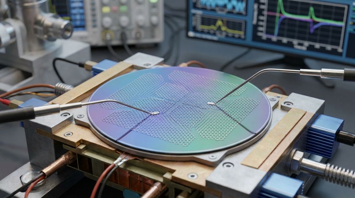
Current non-volatile memory technologies, such as Flash or MRAM, rely on charge storage or magnetic orientation. While effective, they face scaling limits and energy hurdles as we approach the atomic scale. Recent research into rhombohedral multilayer graphene has revealed a phenomenon called chiral superconductivity (CSC). In this state, the material hosts isospin-polarized domains that break time-reversal symmetry.
The engineering breakthrough here is the ability to control these domains using ultra-low current pulses. Unlike standard superconductors, where the state is fixed, rhombohedral graphene allows for reversible switching between states of opposite chirality. This makes it a candidate for a new class of Reconfigurable Chiral Domain Memory (RCDM). In this device, a bit is not represented by a charge, but by the specific configuration of chiral domains within the graphene stack.
The core idea is to use the domain walls between chiral regions as the functional component. The research indicates that these domain walls are highly resistive compared to the superconducting domains themselves. By applying a precise, low-current pulse, we can shift the boundary of a domain, effectively switching the device between a high-resistance state (domain wall present) and a low-resistance state (uniform chiral domain).
This is a "reconfigurable" system. Because the switching is driven by isospin textures rather than massive magnetic fields or high-voltage charge injection, the energy required per bit-flip is orders of magnitude lower than current CMOS or MRAM standards.
Building a prototype requires advanced nanofabrication capabilities. This is not a maker-space project; it is a specialized lab-scale endeavor.
1. Rhombohedral Pentalayer Graphene: This is the most critical and difficult component. You cannot use standard monolayer graphene. You need pentalayer graphene specifically in the rhombohedral stacking sequence. This is typically achieved through precise mechanical exfoliation and controlled stacking of layers.
2. Hexagonal Boron Nitride (hBN): High-quality, atomically flat hBN flakes are required for encapsulation to preserve the delicate electronic properties of the graphene.
3. Silicon/Silicon Dioxide Substrate: A heavily doped silicon substrate is needed to act as a back-gate to provide the required displacement field.
4. Metal Contacts: Gold or Chromium/Gold for electrical leads.
5. Electron-Beam Evaporator: For depositing precise metal contacts.
6. Cryogenic Probe Station: The superconductivity and chiral effects are observed at extremely low temperatures. While the exact temperature for the CSC transition is not specified in the source, we assume a requirement for liquid helium temperatures (approx. 1.5K to 4.2K) for initial prototyping.
7. High-Precision Voltage Source and Picoammeter: To apply the ultra-low current pulses and measure the resulting resistance changes.
1. Substrate Preparation: Clean a Si/SiO2 substrate using standard RCA cleaning procedures to ensure no organic contaminants interfere with the stacking.
2. Graphene Stacking: Using a dry-transfer method (such as the PC or PDMS method), stack five layers of graphene. The stacking must be precisely controlled to achieve the rhombohedral phase. This is the highest risk step in the process. Any deviation in the twist angle between layers will result in a different electronic phase, such as a Mott insulator or a different superconducting state.
3. Encapsulation: Sandwich the pentalayer graphene between two flakes of hBN. This protects the graphene from environmental noise and provides a pristine dielectric environment.
4. Gate Integration: Ensure the Si/SiO2 substrate is ready to act as a back-gate. The device requires a high displacement field to enter the rhombohedral superconducting state.
5. Contact Deposition: Use an electron-beam evaporator to deposit gold contacts at the ends of the graphene flake. Use electron-beam lithography to define the contact geometry.
6. Device Geometry: Design the device as a Hall bar or a simple two-terminal strip. A Hall bar geometry is preferred for testing the transport regimes mentioned in the research.
The goal of the test is to demonstrate reversible switching of the chiral state.
1. Baseline Characterization: Cool the device in a cryostat. Slowly increase the back-gate voltage to reach the displacement field required for the superconducting state. Monitor the resistance.
2. Domain Wall Identification: As the temperature is raised or the gate voltage is tuned, look for the onset of resistance increases that coincide with the proliferation of domain walls. The research suggests that the onset of CSC coincides with the appearance of these walls.
3. Switching Test: Apply a low-current pulse (in the nano-ampere range) across the device. The pulse should be designed to shift the domain wall position.
4. Readout: Measure the resistance immediately after the pulse. A successful switch is indicated by a measurable change in the resistance of the device, representing the transition between different domain configurations.
5. Reversibility Check: Apply a pulse of opposite polarity or different magnitude to see if the device returns to its original resistance state.
1. Stacking Precision: This is the primary failure point. If the layers are not in the rhombohedral configuration, the chiral superconductivity will not emerge.
Mitigation: Use Raman spectroscopy to verify the stacking sequence and electronic properties before proceeding to encapsulation.
2. Thermal Management: The device operates at cryogenic temperatures. Any heat generated by the current pulse, even if small, could disrupt the superconducting state.
Mitigation: Use extremely low duty cycles for the switching pulses and utilize a high-thermal-conductivity substrate to dissipate heat.
3. Signal-to-Noise Ratio: The resistance changes at the domain walls might be subtle.
Mitigation: Use a lock-in amplifier for transport measurements to extract the signal from the noise.
4. Temperature Constraints: The research notes that domain wall proliferation occurs at elevated temperatures relative to the superconducting state.
Assumption: For a prototype, assume a working window between 1K and 10K. If the device does not show switching, the temperature may need to be lowered further to stabilize the superconducting phase.
This guide is based on the research findings of Dutta et al. (2026) regarding reconfigurable chiral superconductivity in rhombohedral multilayer graphene. The engineering application of "reversible switching between states of opposite chirality" is a direct translation of the paper's observation that the chiral domain structure is controllable via ultra-low current. While the paper focuses on the fundamental physics of isospin-polarized domains, this guide treats those domains as the physical basis for a non-volatile, low-power memory bit.
Serious about B2B integration? Test our premium Pulsed Electrical Resistive Carbon Heating turbostratic graphene in your lab. 100g sample packs available now.
Explore More
Research on 30° quasi-periodic twisted bilayer graphene reveals a unique, fractal-like energy structure under magnetic fields, paving the way for novel...

Researchers discover naturally formed graphene sheets and carbon ovals in stingless bee hives, creating a novel emergent material with powerful blue light...

Discover how rippled graphene pores act as fluidic memristors, enabling advanced synaptic functionalities for the next generation of neuromorphic computing.