
Rippled Graphene Pores for Neuromorphic Fluidic Memristive Devices
Discover how rippled graphene pores act as fluidic memristors, enabling advanced synaptic functionalities for the next generation of neuromorphic computing.
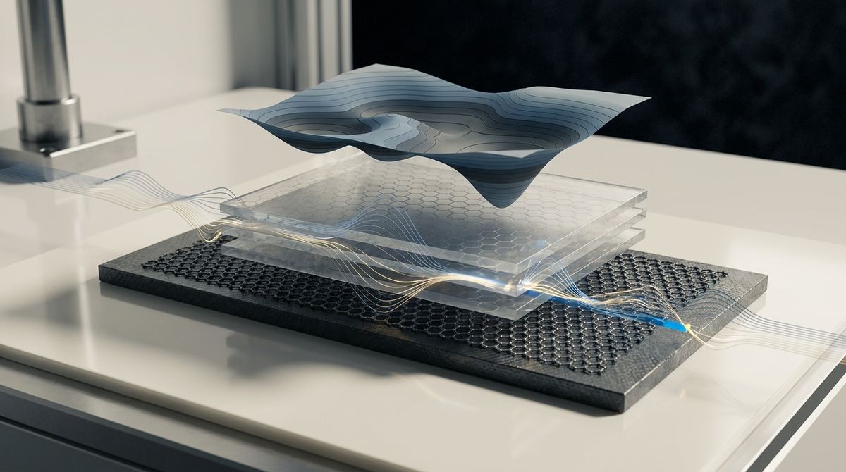
Imagine trying to build a high-tech communication device where the very fabric of the components determines how information travels. In the world of ultra-small electronics, we are moving away from bulky silicon chips and toward single layers of atoms. In this new frontier, the way two different materials touch—their atomic handshake—can change everything from how they conduct electricity to how they process quantum information. This research explores how we can use the symmetry of these atomic layers to "program" the behavior of electrons, potentially leading to a new generation of programmable matter.
For decades, the technology industry has relied on silicon to drive our computers, smartphones, and everything in between. However, silicon is hitting a fundamental physical wall. As engineers try to make transistors smaller to increase speed and reduce power, they encounter the limits of classical physics. At the atomic scale, electrons begin to leak through barriers they should not be able to cross, a phenomenon known as quantum tunneling. This leakage generates heat and prevents transistors from being turned off effectively, creating a massive hurdle for the future of computing.
To solve this, scientists are looking toward two-dimensional, or 2D, materials. Unlike traditional materials, 2D materials are only one or a few atoms thick. This extreme thinness allows for much better control over electronic properties. Graphene, the most famous of these materials, is a single layer of carbon atoms that is incredibly conductive. However, graphene has a major flaw for traditional computing: it lacks a natural bandgap. A bandgap is essentially a "stop" sign for electrons; without it, you cannot easily turn a graphene transistor off.
To fix this, researchers are building van der Waals heterostructures. These are essentially atomic-scale sandwiches where different 2D materials are stacked on top of one another. By placing graphene in contact with other materials, we can "induce" properties into the graphene that it does not possess on its own. The challenge is that controlling this interface is incredibly difficult. If the connection between the layers is too strong or too weak, or if the symmetry of the layers is mismatched, the device will not work as intended. We need a way to precisely tune the "coupling"—the electronic interaction—between the layers to achieve predictable and useful results.
The breakthrough explored in this research centers on a concept called layer-parity. In a crystal, the arrangement of atoms often possesses a certain symmetry. Parity refers to whether a system remains the same or flips its sign when you look at it from the top versus the bottom. In a stack of layers, the number of layers can change this symmetry. For example, a stack with an even number of layers might behave very differently than a stack with an odd number of layers because the electronic environment looks different from the perspective of the middle of the stack.
The researchers investigated a specific material called Nb3Cl8 and stacked it with graphene. They discovered that the way electrons move between the Nb3Cl8 and the graphene is not a fixed property. Instead, it is "parity-dependent." This means that by simply adding or removing a single layer of Nb3Cl8, you can fundamentally change how the two materials communicate electronically. This gives us a new "knob" to turn. Instead of needing to change the chemical composition of the material, we can just change its thickness to control the electronic connection, allowing for much more precise engineering of the device's performance.
To understand how this system works, we have to look at the nature of the van der Waals bond. Unlike most materials where atoms are held together by strong covalent bonds, the layers in a van der Waals heterostructure are held together by much weaker forces. This means the layers are essentially sitting on top of each other with a tiny gap between them. This gap is the stage where the "interfacial coupling" takes place.
When Nb3Cl8 is placed on graphene, the electronic orbitals of the Niobium and Chlorine atoms begin to overlap with the $\pi$-orbitals of the carbon atoms in graphene. This overlap creates a bridge. Electrons can move through this bridge, or their behavior can be influenced by the presence of the other material. The strength and nature of this bridge depend on how the electronic wavefunctions of the two materials line up.
This is where the layer-parity comes into play. In a crystal like Nb3Cl8, the electronic states are distributed in specific patterns throughout the layers. In a single layer, the electron's wavefunction might be symmetric. But once you add a second layer, the symmetry shifts. This change in symmetry alters the "potential landscape" that the graphene electrons feel. If the parity of the layers creates a specific symmetry, it might allow for strong coupling, effectively "injecting" new electronic characteristics into the graphene. If the symmetry is different, the coupling might be much weaker. This ability to manipulate the electronic landscape through symmetry is what makes this system so powerful for advanced materials science.
The research conducted by Hansheng Xu, Yuchen Gao, Xinyue Huang, Weihanzhang Guo, Zhijie Ma, Ziqi Liu, Pinfan Gu, Kenji Watanabe, Takashi Taniguchi, Youguo Shi, and Yu Ye provides a detailed look at this phenomenon. The study focuses on the transition from simple contact to complex electronic coupling as the number of layers in the Nb3Cl8 stack changes.
The findings indicate that the interfacial coupling is highly sensitive to the thickness and the resulting symmetry of the Nb3Cl8 layers. The researchers observed that the electronic state of the graphene is not just slightly modified by the Nb3Cl8, but is fundamentally reshaped depending on whether the number of layers is even or odd. This parity-dependent behavior means that the electronic "handshake" between the materials is not a constant.
Specifically, the researchers were able to map how the electronic structure of the graphene responds to the presence of the Nb3Cl8. They found that the interaction can be tuned, which is a critical requirement for any functional electronic component. By understanding the relationship between layer number and coupling strength, they have provided a roadmap for how to build heterostructures with specific, pre-determined electronic properties. This moves the field from a stage of "trial and error" stacking to a stage of "precision engineering" where the layer count is used as a design parameter.
This discovery is significant because it provides a new method for "tuning" the properties of 2D materials without the need for traditional chemical doping. In conventional semiconductor manufacturing, to change the conductivity of a material, you often have to introduce impurities, a process called doping. This can be messy, difficult to control at the atomic scale, and can create defects that ruin the device's performance.
The ability to use layer-parity to control coupling offers a much cleaner alternative. Because we are using the inherent symmetry of the crystal structure rather than adding foreign atoms, the process is theoretically much more precise. This could lead to the development of "programmable" electronic materials. Imagine a material where you can change its electrical properties simply by stacking it differently or by using an electric field to alter the effective symmetry of the layers.
Furthermore, this research is vital for the development of quantum technologies. Many advanced quantum phenomena, such as topological states or charge density waves, are extremely sensitive to symmetry. If we can control the symmetry of an interface by simply choosing the number of layers, we can create environments that support these delicate quantum states. This is a major step toward building stable, scalable quantum components.
While these findings are a major step forward, there are several significant hurdles that remain before this technology can be used in a consumer device. First, there is the issue of scalability. The research was conducted using high-quality, exfoliated flakes of 2D materials. This is a laboratory technique where a layer is literally "peeled" off a bulk crystal using adhesive tape. While this produces near-perfect crystals, it is not a scalable manufacturing process. To use this in the real world, we would need to find a way to grow these complex, parity-dependent stacks using methods like Chemical Vapor Deposition (CVD) over large areas.
Second, the stability of these heterostructures is a concern. Van der Waals materials are held together by weak forces, making them potentially sensitive to temperature, moisture, and mechanical stress. For a computer chip to last for years, these atomic stacks must be incredibly robust.
Finally, the effects observed in this study were likely measured at specific temperatures or under specific vacuum conditions to avoid interference from environmental noise. For these materials to be commercially viable, the "parity-dependent" effects must be robust enough to function under standard operating conditions. The research is a proof-of-concept that the physics works; the next challenge is making that physics reliable and mass-producible.
The practical implications of this research are vast, spanning from high-performance computing to sensitive scientific instruments. One of the most immediate applications could be in the development of ultra-low-power transistors. If we can use layer parity to precisely control the bandgap and the off-state of a graphene transistor, we could create chips that consume significantly less power than current silicon-based technology, extending battery life in everything from smartphones to satellites.
Another promising area is quantum computing. The ability to engineer the electronic symmetry of an interface is a key requirement for creating qubits—the fundamental building blocks of quantum computers. By using Nb3Cl8/graphene heterostructures, researchers may be able to create more stable environments for quantum states, making the error-prone nature of current quantum computers more manageable.
Finally, this research has profound implications for sensing technology. Because the electronic coupling is so sensitive to the thickness and symmetry of the layers, these materials could be used to create sensors that are incredibly sensitive to external stimuli. A single molecule or a slight change in pressure could disrupt the delicate parity-dependent coupling, leading to a measurable change in the material's electrical properties. This could revolutionize medical diagnostics, environmental monitoring, and security scanning.
If you take away only one idea from this research, let it be this: the number of layers in a 2D material stack can be used as a precision tool to control the electronic "handshake" between materials, offering a new way to engineer the future of electronics through atomic symmetry.
What is a van der Waals heterostructure?
A van der Waals heterostructure is a material stack made by layering different two-dimensional materials on top of each other. Because these materials are only one atom thick, they are held together by weak van der Waals forces rather than strong chemical bonds, allowing us to stack them like thin sheets of paper.
Why is graphene so important in this research?
Graphene is a single layer of carbon atoms that is highly conductive. However, it lacks a bandgap, which means it cannot easily be turned off like a standard transistor. By stacking graphene with other materials, scientists hope to introduce a bandgap or other controlled properties to make it useful for digital electronics.
What does "layer-parity" mean in this context?
Layer-parity refers to the way the physical symmetry of a material changes depending on whether it has an even or odd number of layers. In these quantum systems, changing the number of layers by just one can flip the symmetry of the electronic environment, which fundamentally changes how the material behaves.
What is the role of Nb3Cl8 in this study?
Nb3Cl8 is a transition metal halide that has unique electronic properties. In this research, it acts as a "tuning" layer. When placed on graphene, its atomic structure and symmetry influence how electrons move through the graphene, providing a way to control the graphene's electrical state.
Is this technology ready for use in our phones today?
No, this research is in the fundamental science stage. While the researchers have proven that these effects are real and controllable, the current method of creating these materials (peeling them apart with tape) is not suitable for mass production. Significant work is needed in manufacturing and stability before this reaches consumer products.
The study of Nb3Cl8/graphene van der Waals heterostructures represents a significant leap in our ability to engineer matter at the atomic scale. By moving beyond simple chemical compositions and harnessing the power of structural symmetry and layer parity, researchers are uncovering a new way to control the flow of electrons. While challenges in scalability and stability remain, the ability to "program" the electronic coupling of materials opens a vast new landscape for the next generation of transistors, quantum computers, and ultra-sensitive sensors. As we continue to master the atomic handshake, the limits of what we can achieve with electronic materials will continue to expand.
Serious about B2B integration? Test our premium Pulsed Electrical Resistive Carbon Heating turbostratic graphene in your lab. 100g sample packs available now.
Explore More
Discover how rippled graphene pores act as fluidic memristors, enabling advanced synaptic functionalities for the next generation of neuromorphic computing.

Learn how to use electromechanical responses in gapped graphene to measure electronic temperature and band gaps using traveling flexural waves.

Explore how researchers have discovered viscous electron fluid behavior in cadmium, a breakthrough that could revolutionize the future of nanoelectronics.