
Energy-Gap Control Unlocks Current Oscillations in Graphene
New theoretical research shows how controlling graphene's energy gap under periodic driving can generate high-frequency current oscillations, a key step for...
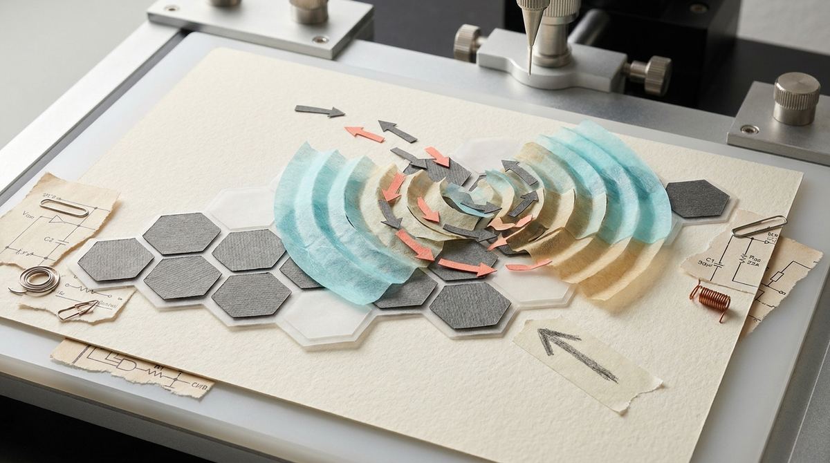
Imagine trying to understand the complex traffic patterns of a major city by only counting the cars that enter and leave its limits. You would know the total volume, but you would have no idea about the traffic jams, the shortcuts drivers are taking, or the areas where flow is smooth and efficient. For decades, this has been the challenge for physicists and engineers studying the movement of electrons through materials. We can measure the current going in and the current coming out, but the intricate dance of electrons inside the device has remained largely hidden. A new theoretical work offers a way to finally see inside the machine, using nanoscale sound waves to create a dynamic map of electron flow.
At the heart of every electronic device is the controlled movement of electrons. Our ability to design faster processors, more efficient solar cells, and more sensitive sensors depends on a deep understanding of how these electrons travel through a material. However, observing this transport directly at the nanoscale is extraordinarily difficult. Conventional electrical measurements provide an average picture, like the city traffic example, obscuring the local details. We know electrons can scatter off defects, get trapped at interfaces, or behave in collectively strange ways, but these phenomena are hard to isolate and visualize. This lack of a high-resolution "electron camera" creates a bottleneck, slowing down the discovery of new materials and the design of novel devices. We are often forced to rely on indirect evidence and theoretical models to guess what is happening inside. This research, by a team including Zi-Qian Zhou, Zhi-Fan Zhang, Cong Xiao, Hua Jiang, and X. C. Xie, tackles this fundamental problem of observation, proposing a non-invasive method to reconstruct the complex dynamics of electrons in real time.
The core concept is elegantly simple: use sound to see electricity. The researchers propose using a type of nanoscale sound wave, known as a Surface Acoustic Wave (SAW), to probe the electronic properties of a material. A SAW is a tiny, high-frequency ripple that travels along the surface of a solid, much like a ripple on the surface of a pond. These waves carry both a physical strain and a localized electric field with them. When a highly conductive two-dimensional material like graphene is placed on the surface where these waves are traveling, the SAW's electric field interacts with the sea of free electrons within the graphene. This interaction gently pushes and pulls on the electrons, causing them to "surf" the acoustic wave. By precisely measuring the tiny electrical currents generated by this "electron surfing" at various points, the researchers theorize that they can work backward using a sophisticated algorithm. This process allows them to reconstruct a detailed, time-resolved map of how the electrons are moving, including their velocity and direction, effectively creating a movie of the electron flow.
The proposed experimental setup relies on a combination of well-understood technologies applied in a novel way. The foundation is a piezoelectric substrate, a type of material that deforms when a voltage is applied to it and, conversely, generates a voltage when it is deformed. Materials like lithium niobate are common choices. On this substrate, a pattern of tiny, interlocking metal fingers called an interdigitated transducer (IDT) is fabricated. When an alternating electrical signal is applied to the IDT, it causes the piezoelectric substrate to expand and contract rapidly, launching a high-frequency Surface Acoustic Wave across the material.
Next, a sheet of high-quality graphene is transferred onto the substrate, directly in the path of the SAW. Graphene is an ideal material for this technique due to its two-dimensional nature and extraordinary electronic mobility. As a single layer of carbon atoms, all of its electrons are essentially on the surface, making them maximally sensitive to the passing SAW. The wave's propagating electric field couples strongly with these mobile charge carriers. This interaction, known as the acousto-electric effect, drags a portion of the electrons along with the wave, generating a measurable direct current. The genius of this work lies in using this effect not just to generate a current, but as a diagnostic tool. By placing multiple electrical contacts around the graphene sheet and measuring the subtle variations in current as the wave passes, a rich dataset is collected. This data contains the "imprint" of how the electrons responded to the SAW's push. A powerful computational algorithm then processes this information to reconstruct the underlying electron velocity field, revealing the hidden pathways, vortices, and traffic jams within the material's electronic system. This approach promises a new frontier in the study of graphene electronics.
Through rigorous theoretical modeling and numerical simulations, the researchers demonstrated the feasibility of their proposed technique. They showed that by analyzing the acousto-electric currents, it is possible to reconstruct the electron dynamics with high fidelity. Their model successfully "inverted" the simulated measurement data to recreate the original electron velocity field, proving the principle of the reconstruction method. More importantly, the work highlights the ability of this technique to uncover "nontrivial" transport phenomena. This term refers to electron behaviors that go beyond simple, straight-line conduction. For example, their simulations could reveal how electrons flow around a defect or impurity in the graphene lattice, showing the formation of microscopic whirlpools or "vortices" of current that would be completely invisible to standard measurement techniques. They could also map out how current constricts or spreads out when moving through channels of varying widths, providing direct visual confirmation of theories that were previously difficult to test. This ability to visualize complex current paths is a significant step forward in understanding the mesoscopic world, where quantum mechanics and classical physics intersect.
This research is significant because it proposes a new and powerful tool for fundamental materials science. It offers a way to bridge the gap between abstract theoretical models of electron transport and tangible experimental data. For decades, scientists have been developing sophisticated theories to describe how electrons should behave in materials like graphene, but verifying these theories directly has been a persistent challenge. This acoustic reconstruction method could provide that verification, allowing researchers to "see" if their models match reality. This deeper understanding has profound implications for future technology. By visualizing how electrons lose energy by scattering off imperfections, engineers could develop strategies to design materials with even lower electrical resistance, leading to more energy-efficient electronics. The ability to map nontrivial and topological electron flows could also accelerate the development of next-generation computing paradigms, such as topological quantum computers, which rely on precisely these kinds of exotic electronic states. This work provides a new lens through which to view the quantum world, potentially revealing new physical phenomena and guiding the design of future graphene applications.
It is crucial to recognize that this paper presents a theoretical framework and computational proof-of-concept. The next, and most significant, hurdle is to build a physical experiment that successfully demonstrates the technique. This presents several practical challenges. Fabricating the device requires precise alignment of the graphene sheet, the piezoelectric substrate, and the electrical contacts. The interface between the graphene and the substrate must be pristine; any impurities or bubbles could disrupt the acoustic wave and ruin the measurement. The signal processing will also be demanding, as the acousto-electric currents are typically very small and must be measured with high precision against a noisy background. Furthermore, the reconstruction algorithm itself may be computationally intensive and will need to be optimized for real-world data. The effectiveness of the technique may also depend on material quality, making it essential to use high-purity materials, such as those derived from a consistent industrial graphene supply. Future work will need to address these engineering challenges and validate the theoretical findings with concrete experimental results.
While this research is at a fundamental stage, its potential long-term applications are broad and exciting. One of the most immediate uses could be as an advanced quality control and characterization tool. Manufacturers of 2D materials could use this technique to map out electronic uniformity and identify defects in their products, ensuring higher quality and yield from their graphene production machinery. In the realm of electronics, the principles could be adapted to create new types of highly sensitive detectors. For instance, if a single molecule lands on the graphene surface, it would slightly alter the local electron flow; this tiny disturbance could be detected and mapped by the acoustic wave system, forming the basis for an incredibly sensitive chemical or biological sensor. Furthermore, the interaction between SAWs and electrons is already used in radio-frequency (RF) signal processing components found in smartphones. A deeper understanding and control of this interaction, as provided by this research, could lead to more efficient and compact filters and signal modulators for next-generation communication systems.
If there is one key takeaway from this work, it is this: scientists have developed a theoretical blueprint for using nanoscale sound waves as a "sonar" to map the intricate flow of electrons inside a material like graphene. This technique promises to turn a hidden quantum dance into a visible movie, opening a new window for designing the materials and devices of the future.
What is a surface acoustic wave in this context?
A surface acoustic wave, or SAW, is a high-frequency mechanical vibration that travels along the surface of a solid material. In this research, it is generated on a special piezoelectric crystal by applying an electrical signal. You can think of it as a precisely controlled, nanoscale ripple that carries both a physical strain and an associated electric field, which is used to interact with the electrons in the graphene.
Why is graphene a good material for this research?
Graphene is exceptionally well-suited for this technique for several reasons. First, it is a two-dimensional material, meaning all its atoms and its free-moving electrons are confined to a single plane. This makes the electrons highly exposed and sensitive to the electric fields from the surface acoustic wave. Second, graphene boasts incredibly high electron mobility, meaning its electrons can move long distances without being scattered, which results in a strong and clear signal from the acousto-electric interaction.
What does "reconstructing electron dynamics" mean?
Reconstructing electron dynamics means creating a detailed map or even a video of how electrons are moving inside the material. Instead of just getting a single number for the total current, this technique aims to determine the velocity—both the speed and direction—of electrons at many different points across the graphene sheet. This allows researchers to visualize the complete flow pattern, including complex features like eddies or choke points.
Is this technology a product I can buy today?
No, this technology is currently at the theoretical and computational research stage. The paper provides the scientific foundation and a "recipe" for how such a system could work, but it has not yet been built and tested in a physical experiment. Significant engineering and experimental validation are required before this could become a commercial characterization tool or be integrated into a consumer device.
How is this different from a normal transistor?
A normal transistor acts as a switch or an amplifier, controlling the overall flow of current from a source to a drain by applying a voltage to a gate. Its purpose is to control the amount of current. This acoustic wave technique, on the other hand, is not designed to be a switch. Its purpose is to be a measurement tool—a diagnostic instrument used to observe and map how the current is already flowing within a material, providing a level of detail that a simple transistor cannot.
The proposal to use acoustic waves for the reconstruction of electron dynamics represents a creative and powerful convergence of physics and engineering. By turning the well-known acousto-electric effect into a high-resolution imaging technique, this research paves the way for a new era of materials characterization. While experimental validation remains a critical next step, the theoretical groundwork laid by this study is a vital contribution. It provides a clear path toward visualizing the fundamental behaviors that govern the electronic devices we depend on. This ability to "see" the electron flow is not merely an academic curiosity; it is a prerequisite for the intentional design of next-generation materials and the continued advancement of technology at the quantum scale.
Serious about B2B integration? Test our premium Pulsed Electrical Resistive Carbon Heating turbostratic graphene in your lab. 100g sample packs available now.
Explore More
New theoretical research shows how controlling graphene's energy gap under periodic driving can generate high-frequency current oscillations, a key step for...

Research on magic-angle twisted bilayer graphene reveals a new geometric component of superfluid stiffness, a key property for robust Kekulé superconductivity.

Explore the Josephson effect in graphene Corbino disks, a breakthrough offering gate-tunable control over quantum supercurrents for next-gen sensors and...