
Mesoscopic Josephson effect in graphene disk at magnetic field
Explore the fascinating intersection of superconductivity and graphene as researchers investigate how mesoscopic disks respond to magnetic fields through the Josephson effect.
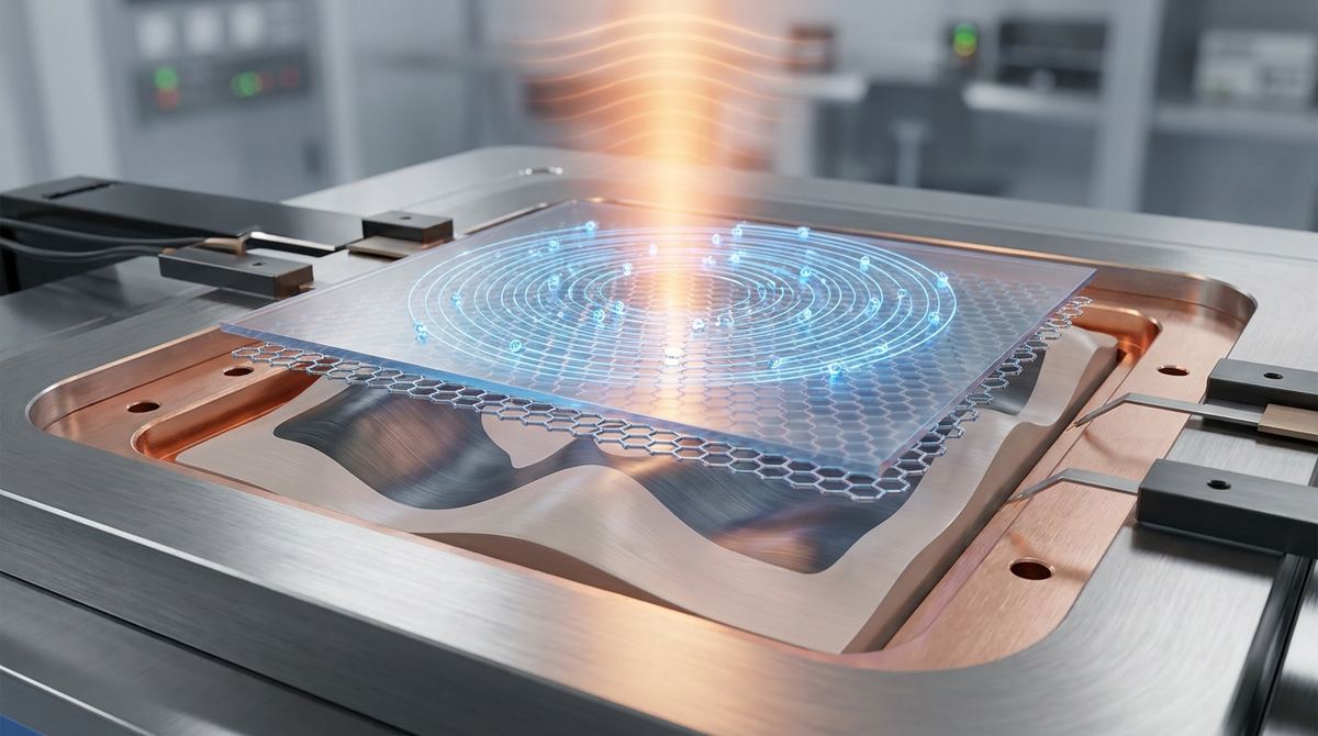
Imagine you are trying to inspect a high-speed highway to find a single, microscopic crack that might cause a vehicle to swerve. From a helicopter, the road looks perfectly smooth, but to the driver, that tiny crack is a massive obstacle. For the engineers building the next generation of ultra-fast computers and lightning-fast communication networks, graphene is that highway. It is a material that promises to carry signals at incredible speeds, but there is a catch. Even the slightest impurity or tiny bump in the surface can disrupt the flow of electrons, causing errors or slowing down the device. To truly master graphene, we need to see these microscopic obstacles with absolute precision, without destroying the very material we are trying to study.
Graphene, a single layer of carbon atoms arranged in a hexagonal lattice, is a superstar in the world of materials science. Because it is incredibly thin and possesses unique electronic properties, it has the potential to revolutionize everything from smartphone processors to quantum computers. However, graphene is notoriously sensitive to its environment. When a single layer of graphene is placed on a standard substrate, like silicon dioxide, the "messiness" of that substrate—the atoms that aren't perfectly aligned or the stray electrical charges trapped in the surface—interferes with the graphene. This interference is known as charge impurity scattering.
This scattering acts like friction for electrons, dragging down their mobility and making it difficult to predict how a device will actually perform. Furthermore, standard measurement techniques often provide an "average" view of the material. They tell us how much electricity flows through a large area, but they cannot tell us if that flow is being disrupted by a single tiny defect in one specific corner. This lack of spatial resolution is a major roadblock. If we cannot see exactly where and why electrons are slowing down, we cannot engineer better, more reliable graphene-based components. We are essentially trying to optimize a complex machine while only being able to see its overall output rather than its internal mechanics.
The researchers have proposed a way to look at these microscopic details using a combination of two powerful tools: terahertz light and magnetism. Terahertz radiation is a type of electromagnetic wave that sits in the frequency spectrum between common microwaves and infrared light. This frequency range is special because it matches the natural energy scales at which electrons move within graphene. By using this light, we can "nudge" the electrons and watch how they respond.
When we add a magnetic field into the mix, something fascinating happens. The magnetic field exerts a force on the moving electrons, forcing them to move in circular orbits rather than straight lines. This movement is called cyclotron motion. The frequency at which the electrons spin in these tiny circles is directly linked to the number of electrons present and how easily they can move. By scanning a tiny, focused beam of terahertz light across the graphene while a magnetic field is applied, we can map out exactly where the electrons are moving smoothly and where they are getting stuck. This technique, called terahertz magneto-nanoscopy, allows us to create a high-resolution map of the material's electrical landscape at the nanoscale.
To achieve the level of precision required for this research, the team—including Richard H. J. Kim, Sunwoong Yang, Taehoon Kim, Samuel J. Haeuser, Joong-Mok Park, Randall K. Chan, Thomas Koschny, Young-Mi Bahk, Sung Ju Hong, and Jigang Wang—focused on a sophisticated setup known as encapsulation. Instead of leaving the graphene exposed to the air or a messy substrate, they "sandwiched" the monolayer graphene between two extremely clean layers of hexagonal boron nitride, or hBN.
This encapsulation is a critical engineering step. Hexagonal boron nitride is an insulator that is structurally very similar to graphene but is atomically smooth and lacks the stray charges that plague other substrates. By placing the graphene in this protective hBN environment, the researchers effectively isolate it from the outside world. This reduces the frequency of electron-impurity collisions, allowing the graphene to reach its theoretical maximum performance. This "clean" environment is essential because it ensures that the signals being measured are a result of the graphene's intrinsic properties rather than noise from the surroundings.
Once the encapsulated sample is prepared, the magneto-nanoscopy process begins. A pulsed terahertz beam is focused onto a specific point on the graphene surface. This pulse provides the necessary energy to excite the electrons into their cyclotron orbits. When a perpendicular magnetic field is applied, the Lorentz force pushes the electrons into these circular paths. The frequency of these orbits, known as the cyclotron resonance frequency, is the key piece of data. Because the frequency depends on the local density of the electrons, any variation in density or any local obstacle that disrupts the orbit will change the signal detected by the sensors. By moving the terahertz beam across the surface in a controlled pattern, the researchers can reconstruct a highly detailed map of the local conductivity and carrier density.
Through this advanced nanoscopy technique, the researchers were able to observe the local variations in electron transport that are invisible to conventional methods. They found that even in highly optimized, encapsulated samples, there are subtle variations in the electrical landscape. The ability to resolve these variations at the nanoscale provides a direct view of how charge carriers behave in the presence of localized potentials.
The research demonstrated that terahertz magneto-nanoscopy can effectively distinguish between the intrinsic properties of the graphene and any remaining local defects. By observing the cyclotron resonance, the researchers could determine the local mobility—essentially a measure of how "fast" an electron can travel before being scattered—with unprecedented spatial resolution. This allows for a clear understanding of how the local environment, even within an encapsulated structure, influences the macroscopic electrical performance of the material. Essentially, the study proved that we can move beyond seeing the "average" behavior of graphene and start seeing its actual, localized reality.
This research is a significant step forward for the field of two-dimensional materials science. The ability to map local electronic properties at the nanoscale means that engineers can move from trial-and-error fabrication to precision engineering. If we can see exactly where a device is failing at the molecular level, we can design ways to mitigate those specific issues.
Furthermore, this technique addresses one of the most significant challenges in high-frequency electronics: the need for ultra-fast, high-efficiency devices. As we move toward higher frequency communication standards, such as 6G and beyond, the materials used must be able to operate at terahertz frequencies without losing signal integrity. Understanding how electrons move in the terahertz regime is not just an academic exercise; it is a fundamental requirement for building the hardware that will power the next generation of global telecommunications.
While this research represents a major technical achievement, several challenges remain before this technology can be used in mass-produced electronics. First, the process of encapsulating graphene between layers of hBN is incredibly complex and time-consuming. It requires specialized laboratory equipment and extreme care to ensure that no impurities are introduced during the transfer process. Scaling this up to a factory setting for large-scale chip manufacturing remains a significant engineering hurdle.
Second, the magneto-nanoscopy setup itself is highly sophisticated and requires precise synchronization between the terahertz pulses and the magnetic field measurements. Current systems are largely confined to specialized research laboratories and are not yet portable or cost-effective for standard industrial quality control. Finally, while the technique provides a map of electronic behavior, it does not automatically tell us how to fix the underlying defect. There is a gap between observing a problem through nanoscopy and developing the materials science techniques required to eliminate those defects during the growth of the graphene itself.
The implications of terahertz magneto-nanoscopy extend into several high-tech industries. In the realm of telecommunications, this research supports the development of ultra-high-speed transistors and modulators that can operate at frequencies far beyond current silicon-based technology. This could lead to much faster data transmission and lower latency in mobile networks.
In the field of quantum computing, the ability to map electronic movement at the nanoscale is vital. Many quantum bits, or qubits, rely on the precise control of single electrons or the movement of charge carriers in low-dimensional materials. Understanding the local landscape of the material is essential for creating stable, high-fidelity qubits that are protected from environmental noise.
Additionally, high-speed sensing technology stands to benefit. Terahertz sensors are used in security, medical imaging, and non-destructive testing. Using graphene-based terahertz components could lead to sensors that are much more sensitive and capable of detecting much smaller objects or chemical signatures than current technologies allow.
If you remember only one thing from this research, let it be that to build the future of ultra-fast technology, we must be able to see the microscopic imperfections that govern how electrons move in advanced materials like graphene.
How does graphene differ from traditional silicon? Graphene is a single layer of carbon atoms that is incredibly thin and highly conductive. Unlike silicon, which is a bulk material used in three-dimensional structures, graphene is two-dimensional, meaning its electrons are confined to a single plane, which leads to much faster movement and unique electronic properties.
Why is it necessary to "sandwich" graphene in hBN? Graphene is extremely sensitive to its surroundings. If it is left exposed, it picks up impurities and electrical noise from the air or the material it is sitting on. Encapsulating it in hexagonal boron nitride provides a clean, atomically flat environment that allows the graphene to perform at its theoretical best, making it easier for scientists to study its true properties.
What exactly is terahertz radiation? Terahertz radiation is a form of electromagnetic energy that exists between the frequencies of microwaves and infrared light. It is useful for studying electronics because its energy levels correspond closely to the energy levels of the electrons in materials like graphene, allowing us to probe their behavior very effectively.
What is the purpose of applying a magnetic field during these measurements? When a magnetic field is applied, it exerts a force on moving electrons, causing them to move in circles rather than straight lines. The frequency of these circles, called cyclotron resonance, tells scientists a lot about how many electrons are present and how much they are being hindered by defects or impurities.
Can this research be used to make better computers immediately? Not quite yet. While this research provides a way to see and understand the problems in graphene, we are still in the stage of perfecting the measurement techniques and the fabrication methods. It is a foundational step that will eventually lead to better manufacturing processes for the high-speed components used in future computers.
The work conducted by the research team provides a vital window into the microscopic world of encapsulated graphene. By combining the precision of terahertz radiation with the physics of magnetic cyclotron motion, they have demonstrated a powerful method for mapping the local electrical landscape of two-dimensional materials. While challenges in manufacturing and scalability remain, this ability to visualize the movement of electrons at the nanoscale is a fundamental requirement for the next era of high-frequency electronics, quantum computing, and ultra-fast communications. As we continue to push the limits of what materials can do, tools like terahertz magneto-nanoscopy will be essential in turning the promise of graphene into a reality.
Serious about B2B integration? Test our premium Pulsed Electrical Resistive Carbon Heating turbostratic graphene in your lab. 100g sample packs available now.
Explore More
Explore the fascinating intersection of superconductivity and graphene as researchers investigate how mesoscopic disks respond to magnetic fields through the Josephson effect.

A practical guide for quantum hardware startups and research labs to prototype bilayer graphene quantum dots for qubit development, based on recent noise characterization studies.
![792. Exact results for the Hubbard model on bipartite lattices in spatial dimensions $d>1$: Seven theorems from the full [SU(2)$\times$SU(2)$\times$U(1)]/$\mathbb{Z}_2^2$ symmetry](/_next/image/?url=https%3A%2F%2Fcdn.sanity.io%2Fimages%2Ft9t7is4j%2Fproduction%2Fb3dd0f5b84ae321728ba826fbf875a482fefd050-1376x768.jpg%3Frect%3D6%2C0%2C1365%2C768%26w%3D400%26h%3D225%26q%3D75%26auto%3Dformat&w=3840&q=75)
A deep dive into the mathematical breakthroughs of J. M. P. Carmelo, exploring how exact symmetry-based theorems solve the fundamental mysteries of electron behavior in bipartite lattices.