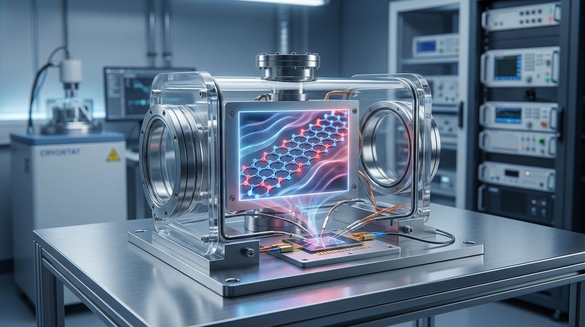
The Concept: Spin-Caloritronics and the Thermal Spin Gate
In the race to move beyond traditional silicon-based electronics, spin-caloritronics has emerged as a high-potential field. While standard electronics rely on the movement of charge (electrons), spin-caloritronics utilizes the spin degree of freedom of electrons, driven by temperature gradients. This approach promises significantly lower power consumption because it can potentially generate pure spin currents—where spin moves without a corresponding flow of charge—thereby eliminating Joule heating.
The research by Luo, Xie, and Wu provides a theoretical blueprint for a device that can control this spin current. The core mechanism involves Zigzag Graphene Nanoribbons (ZGNRs). Unlike standard graphene, ZGNRs possess unique magnetic properties at their edges. When these edges are doped with periodic patterns of Boron (B) and Nitrogen (N), an internal electric field is created. This field allows an engineer to switch the magnetic state of the ribbon between an Antiferromagnetic (AF) state and a Ferromagnetic (FM) state using an external electric field.
In the AF state, the magnetic moments at the two edges are opposite, resulting in zero net spin current. In the FM state, the moments are aligned, allowing a spin current to flow. By applying a temperature gradient across the ribbon, you create a thermal spin current that can be switched on and off electrically. This is essentially a thermal spin-current gate.
The Device: A Thermal Spin-Current Gate
The goal for a prototype is to build a device that demonstrates the transition from an AF state to an FM state to control spin-current flow.
The device architecture consists of a ZGNR channel with periodic B-N doping, placed on a substrate that allows for electrical gating. A heavy metal layer, such as Platinum (Pt), is deposited on top of the nanoribbon. This layer acts as the detector. When the ZGNR produces a spin current, the spin current diffuses into the Platinum layer. Through the Inverse Spin Hall Effect (ISHE), this spin current is converted into a measurable transverse voltage.
Required Materials and Substrates
To attempt a laboratory-scale prototype, you will need the following materials. Note that many of these require advanced nanofabrication facilities.
1. Substrate: Hexagonal Boron Nitride (hBN) is the preferred substrate for high-performance graphene devices due to its atomically smooth surface and lack of dangling bonds, which minimizes charge scattering.
2. Active Material: Zigzag Graphene Nanoribbons (ZGNRs). The ribbons must have well-defined zigzag edges.
3. Dopants: Boron and Nitrogen precursors for Chemical Vapor Deposition (CVD).
4. Detection Layer: A thin film of Platinum (Pt) or Tantalum (Ta) for the Inverse Spin Hall Effect detection.
5. Electrodes: Gold (Au) or Palladium (Pd) for electrical contacts.
6. Thermal Control: Micro-heaters made of Platinum (Pt) or Nickel-Chromium (NiCr) to create the temperature gradient.
7. Gate Dielectric: A thin layer of Hafnium Oxide (HfO2) or Aluminum Oxide (Al2O3) if using a back-gate configuration.
Prototype Fabrication Workflow
Building this device is an advanced engineering task. The following steps outline a theoretical workflow for a research lab or startup.
1. Substrate Preparation: Clean the hBN substrate using standard sonication and plasma cleaning protocols to ensure a pristine surface.
2. Nanoribbon Synthesis: This is the most critical and difficult step. You must grow ZGNRs with specific zigzag edges. While bottom-up chemical synthesis using precursor molecules is the most precise method for controlling edge geometry, CVD on metal catalysts is a more scalable engineering approach.
3. Doping Implementation: The research relies on periodic B and N substitution. In a practical setting, achieving perfect periodicity is an engineering assumption. For a first prototype, aim for a controlled doping concentration of approximately 2% to 5% atomic ratio. You can attempt this by introducing Borane (BH3) and Ammonia (NH3) during the CVD growth process.
4. Device Patterning: Use Electron Beam Lithography (EBL) to define the nanoribbon channel and the placement of the heavy metal detection layer.
5. Metal Deposition: Use Electron Beam Evaporation to deposit the Platinum detection layer and the Gold/Palladium contact electrodes.
6. Gate Integration: Deposit a dielectric layer and a top-gate electrode to allow for the application of the external transversal static electric field required to switch the magnetic states.
7. Thermal Integration: Integrate micro-heaters at one end of the device to establish a controlled temperature gradient across the ribbon.
Measurement and Testing Protocol
Once the prototype is fabricated, the following test plan should be executed to validate the spin-caloritronic effect.
1. Structural Characterization: Use Scanning Tunneling Microscopy (STM) and Raman Spectroscopy to confirm the zigzag edge geometry and the presence of B and N dopants.
2. Thermal Gradient Application: Apply power to the micro-heaters to create a temperature gradient (Delta T). For a cautious starting range, aim for a Delta T of 50K to 100K.
3. Spin-Current Detection: Monitor the voltage (V_ISHE) across the Platinum layer. If the device is working, a voltage should appear when a temperature gradient is present.
4. Magnetic State Switching: Apply a varying voltage to the top-gate electrode. As the gate voltage changes, the internal electric field will modulate the magnetic coupling. You are looking for a sharp change in the measured V_ISHE as the ribbon transitions from the AF state (zero voltage) to the FM state (detectable voltage).
5. Temperature Sensitivity: Repeat the measurement across a range of temperatures to determine the operational window of the device.
Engineering Challenges and Risk Mitigation
This device is at the frontier of materials science, and several risks must be managed.
1. Edge Roughness: The magnetic properties of ZGNRs are highly dependent on the perfection of the zigzag edges. Any atomic-scale roughness can destroy the magnetic order. Mitigation: Use bottom-up molecular synthesis rather than top-down etching to ensure edge precision.
2. Doping Precision: The research assumes periodic B and N substitution. In practice, random doping may occur. Mitigation: If random doping occurs, the device may still function but with lower efficiency. Focus on optimizing the precursor gas ratios during CVD to increase the likelihood of periodic patterns.
3. Signal-to-Noise Ratio: The voltage generated via the Inverse Spin Hall Effect in a nanoribbon is extremely small (microvolts or nanovolts). Mitigation: Use high-precision, low-noise lock-in amplifiers and cryogenic-capable measurement setups to isolate the signal from thermal noise.
4. Thermal Management: High temperature gradients can cause mechanical stress or damage the device. Mitigation: Use hBN as a substrate to help dissipate heat and prevent localized hot spots that could degrade the graphene lattice.
Scientific Basis and Limitations
This guide is based on the theoretical findings of Luo, Xie, and Wu (2026). The research proves that B-N doping creates an internal electric field that can switch the ground state of ZGNRs between AF and FM configurations. This switching is the fundamental mechanism that allows for the control of a pure thermal spin current.
It is important to note that while the research suggests room-temperature operation is possible, the practical implementation in a lab setting may require lower temperatures to stabilize the magnetic states and improve signal detection. The transition from a theoretical model to a physical prototype is a significant leap, particularly regarding the precision of the B-N doping pattern and the maintenance of perfect zigzag edges.