
AI Designs Graphene Nanocomposite for Interstellar Spacecraft Shielding
Researchers use AI to accelerate the discovery of new materials, identifying a graphene-boron nitride composite for interstellar spacecraft shielding.
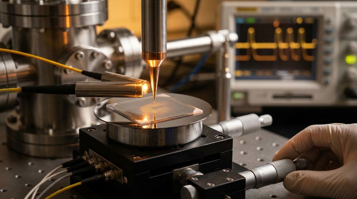
Imagine you are trying to map a sprawling, complex city using only a satellite that can see the streets and buildings, but is completely blind to anything that moves vertically, like elevators or rising smoke. In the world of nanotechnology, scientists are trying to map the vibrations of individual atoms within a single layer of material. These vibrations act like a unique fingerprint, telling us exactly what the material is and how it is being used. For a long time, our mathematical models for this process were only looking at the horizontal movements of atoms, ignoring the vertical, or out-of-plane, movements. This oversight meant that our maps of the atomic world were incomplete. The recent work by Raul Corrêa, Luiz G. Cançado, and Ado Jorio provides the missing dimension, creating a complete mathematical map that accounts for every direction of atomic motion.
To understand why this research is vital, we must first understand the limitations of standard light-based observation. Traditional Raman spectroscopy is a powerful technique used to identify materials by measuring how they scatter light. When a laser hits a material, the light interacts with the molecular vibrations, causing a shift in color (energy) that reveals the material's identity. However, standard Raman spectroscopy is limited by the diffraction limit of light. This means that even with a very fine laser, you cannot see details much smaller than the wavelength of the light itself, which is hundreds of nanometers across. This is far too large to see the individual features or defects in a single layer of graphene or other two-dimensional materials.
This is where Tip-Enhanced Raman Spectroscopy, or TERS, comes in. TERS solves this problem by using a specialized, incredibly sharp metallic tip, often attached to an atomic force microscope. This tip acts like a tiny, ultra-powerful antenna. When the laser hits the tip, it creates a massive concentration of electromagnetic energy at the very point of the needle. This localized hotspot allows scientists to achieve nanometer-scale resolution, essentially bypassing the diffraction limit.
The problem that researchers like Corrêa, Cançado, and Jorio addressed is that existing theoretical models for TERS were incomplete. Most models focused on the in-plane Raman response. This means they could predict how atoms move left-to-right or forward-and-back within the sheet. However, 2D materials are not always perfectly flat, and many of their most important vibrations involve atoms moving up and down, perpendicular to the surface. If a theory only accounts for in-plane vibrations, it cannot accurately interpret the experimental data collected during TERS measurements. This discrepancy can lead to incorrect conclusions about the material's chemical composition, its structural integrity, or the presence of defects. Without a complete theory, we are essentially trying to interpret a three-dimensional reality through a two-dimensional lens.
The key idea presented by the researchers is to unify the mathematical description of how a TERS tip interacts with a 2D material by including the out-of-plane component of the Raman signal. Instead of treating the material as a flat sheet where only side-to-side movements matter, the new theory treats the material as a dynamic, three-dimensional system where vertical movements are equally important to the signal. By incorporating these out-of-plane responses into the equations, the researchers have provided a way to accurately predict and interpret the full spectrum of light scattering that occurs when a nanoscopic tip probes a single layer of atoms. This allows for a much more precise understanding of how the material is behaving at its most fundamental level.
To understand how this system works, we have to look at the physics of the interaction between light, the metallic tip, and the 2D material. When a laser is directed at the TERS setup, the light interacts with the metallic tip, inducing a phenomenon known as surface plasmon resonance. This resonance causes the electrons in the metal to oscillate collectively, creating an incredibly intense and highly localized electromagnetic field at the apex of the tip. This is the "hotspot" mentioned earlier.
When this intense field hits the 2D material, it creates a strong electric field gradient. This gradient is essential because Raman scattering is a nonlinear process that depends not just on the strength of the field, but on how quickly that field changes over a tiny distance. This field interacts with the polarizability of the 2D material. Polarizability is a measure of how much the electron cloud of an atom or molecule can be distorted by an external electric field.
In a 2D material like graphene, the atoms are arranged in a specific lattice structure. When the concentrated field from the TERS tip hits this lattice, it pushes and pulls on the electrons, which in turn causes the atoms to vibrate. These vibrations, known as phonons, occur in different modes. Some modes involve atoms moving within the plane of the sheet, while others involve atoms moving out of the plane.
The mathematical complexity arises because the tip's field is not uniform. It is extremely concentrated at the tip and drops off rapidly as you move away. The researchers had to develop a framework that accounts for how this non-uniform field interacts with the full three-dimensional polarizability tensor of the material. By including the out-of-plane components, the theory can now account for how the vertical movement of atoms changes the way the material scatters light. This includes how the vertical movement affects the local electron density and how the tip's field strength changes as the atoms move up and down. This comprehensive approach ensures that the simulated signal matches what a real-world researcher would see under the microscope.
The researchers successfully developed a theoretical framework that incorporates the out-of-plane Raman response into the TERS signal. This means they have created a complete mathematical model that can describe the Raman scattering of 2D materials with much greater accuracy. Specifically, the theory shows that the out-of-plane vibrational modes contribute significantly to the total signal, especially when the tip is in very close proximity to the material or when the material has structural irregularities.
One of the most significant findings is that ignoring the out-of-plane response leads to a fundamental misunderstanding of the material's symmetry and its interaction with the tip. The theory demonstrates that the out-of-plane mode is not just a minor correction but a vital component for a complete description of the Raman tensor. This work provides the mathematical groundwork for researchers to distinguish between different types of vibrations, such as those caused by intentional chemical modifications versus those caused by accidental defects like wrinkles or vacancies in the lattice. Essentially, the research proves that a complete theory must be a three-dimensional theory to be useful in the real world.
This research matters because it provides the foundational tools needed for the next generation of nanotechnology. As we move toward smaller and more efficient electronic devices, we are increasingly relying on 2D materials like graphene and transition metal dichalcogenides (TMDs). To manufacture these materials reliably, we need to be able to inspect them at the atomic scale with absolute certainty.
If a manufacturer is trying to determine if a layer of graphene has a specific chemical defect, they need to know exactly what that defect's vibrational signature looks like. Without a theory that includes out-of-plane movements, they might misidentify a harmless ripple in the material as a critical chemical defect, or vice versa. This could lead to massive waste in high-end semiconductor manufacturing. By providing a complete theoretical model, this research allows for more accurate characterization, leading to better quality control and more predictable material behavior in real-world devices. Furthermore, it enables a deeper scientific understanding of how 2D materials interact with their environment, which is crucial for developing new types of sensors and quantum computing components.
While this research is a major theoretical breakthrough, it is important to note that it is a theoretical framework, not a new experimental tool. The researchers have provided the mathematical roadmap, but the physical implementation of these theories in a laboratory setting remains a complex task.
Current TERS experiments are extremely sensitive to environmental noise, temperature fluctuations, and the exact geometry of the tip. While the theory accounts for the out-of-plane response, experimentalists still face the massive challenge of maintaining the ultra-stable conditions required to observe these subtle signals. Additionally, while the theory is robust for single layers of 2D materials, applying it to multi-layered structures or more complex heterostructures (where different 2D materials are stacked) will require even more complex mathematical expansions. The next step in this scientific journey is to see how these theoretical predictions hold up in high-precision, real-world experimental environments.
The implications for real-world technology are vast and span several industries. In the semiconductor industry, the ability to accurately map 2D materials could revolutionize how we build the next generation of transistors and interconnects. As devices shrink toward the atomic scale, the ability to detect out-of-plane defects becomes a necessity for maintaining yield and performance.
In the field of chemical sensing, TERS is used to detect single molecules. A more complete theory allows for much more precise identification of these molecules, enabling the creation of highly sensitive biosensors that could detect diseases at much earlier stages by observing the unique vibrational signatures of biomarkers. Finally, in material science research, this theory will allow for the exploration of new "van der Waals heterostructures," where different 2D materials are layered together like LEGO bricks. Understanding how these layers interact—including their vertical vibrations—is key to designing new materials with customized electrical, optical, and mechanical properties.
If you remember only one thing from this research, let it be this: to truly understand the microscopic world, our mathematical models must account for every dimension of movement, because in the world of 2D materials, the "up and down" is just as important as the "left and right."
What is the main purpose of TERS?
TERS, or Tip-Enhanced Raman Spectroscopy, is a highly advanced imaging technique that uses a sharp, metallic tip to amplify the light scattering from a tiny area. This amplification allows scientists to see the chemical and structural details of materials at a scale much smaller than what standard light microscopy allows.
Why do scientists care about out-of-plane vibrations?
Most 2D materials are not perfectly flat; they have ripples, wrinkles, or chemical attachments that move atoms up and down. Because these vertical movements significantly affect how light interacts with the material, scientists must include them in their calculations to accurately identify the material and its defects.
How does this research help with making better electronics?
As electronics get smaller, we use thinner materials like graphene. To ensure these materials work correctly in a chip, we need to be able to detect any imperfections. This research provides the math needed to accurately identify those imperfections, which helps in manufacturing more reliable and efficient electronic components.
Is this theory ready to be used in a factory today?
Not quite. This is a theoretical development that provides the mathematical framework for understanding the process. While it is a vital step forward, experimentalists still need to refine their physical instruments and testing methods to match the precision described in these new equations.
What are 2D materials?
Two-dimensional materials are materials that are only one or a few atoms thick. Examples include graphene, which is a single layer of carbon atoms. These materials are unique because their properties, such as how they conduct electricity, are very different from the same material in a bulk, three-dimensional form.
The transition from traditional Raman spectroscopy to Tip-Enhanced Raman Spectroscopy has opened a new window into the nanoworld. However, that window was previously limited by an incomplete understanding of how light interacts with the vertical movement of atoms. The work of Raul Corrêa, Luiz G. Cançado, and Ado Jorio has fundamentally strengthened this window. By providing a comprehensive theory that includes the out-of-plane Raman response, they have given the scientific community a complete and accurate tool for interpreting the vibrational signatures of 2D materials. This theoretical advancement is a crucial step toward the precise characterization and industrial application of the next generation of nanomaterials.
Serious about B2B integration? Test our premium Pulsed Electrical Resistive Carbon Heating turbostratic graphene in your lab. 100g sample packs available now.
Explore More
Researchers use AI to accelerate the discovery of new materials, identifying a graphene-boron nitride composite for interstellar spacecraft shielding.

In BN-encapsulated graphene, the ultimate limit on electron speed is not graphene itself, but remote phonon scattering from the insulating layers that...

Determinant Monte Carlo simulations are key to materials science but fail at low temperatures. New research offers a stable algorithm, enabling accurate...