
Graphene's Wave-to-Current Conversion: A New Path to Energy Harvesting
Researchers predict a new physical effect in gapless Dirac materials like graphene, where propagating waves can induce a direct DC current without a p-n...
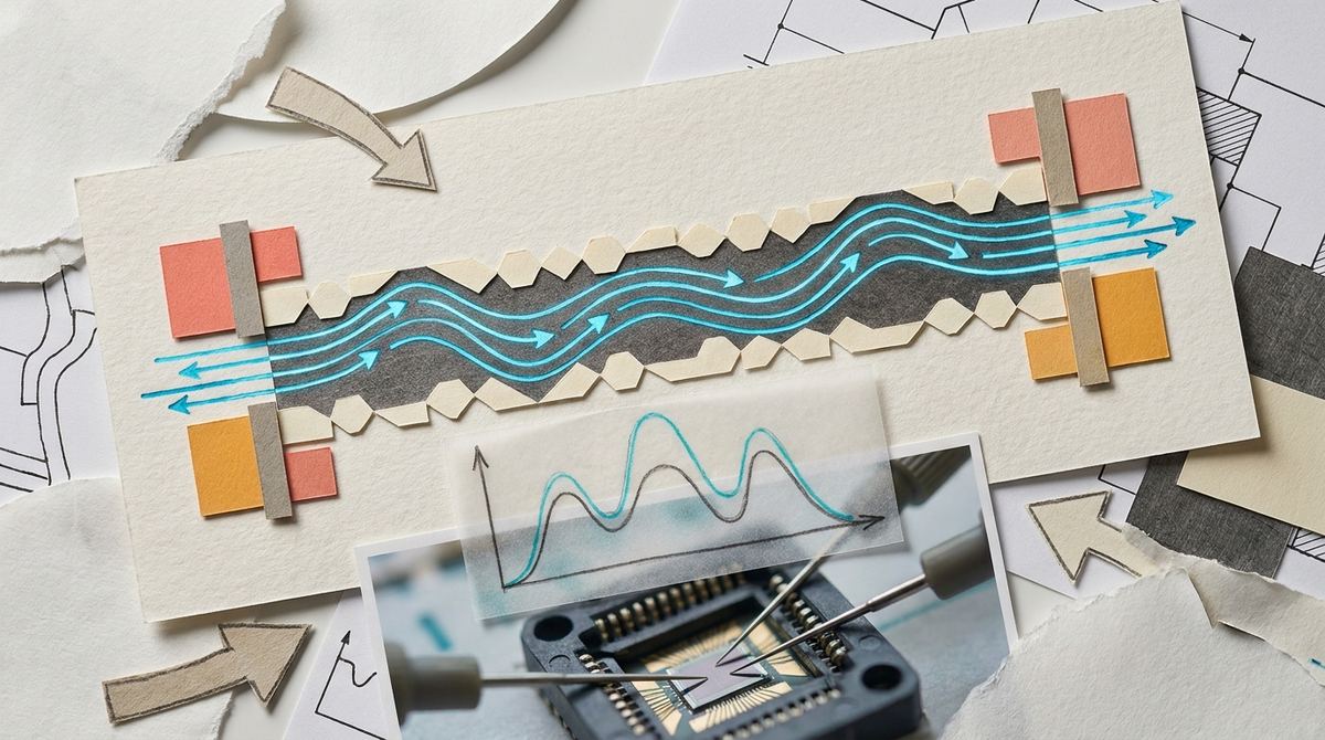
As the world pushes toward the absolute limits of silicon-based computing, scientists are looking toward much smaller, much faster materials to sustain the digital revolution. Graphene, a single layer of carbon atoms, has long been the superstar of this search due to its incredible speed and conductivity. However, as we try to shrink graphene into tiny channels called nanoribbons to make smaller transistors, we run into a massive problem: the edges. When you cut a material into such a small width, the atoms at the edges become the dominant force, often causing electrons to crash into the boundaries and get stuck. This phenomenon, known as localization, effectively kills the material's ability to carry a current. Recent breakthroughs are now exploring how we might use complex, non-repeating patterns along these edges to guide electrons instead of blocking them. This groundbreaking work, conducted by Diego B. Fonseca, Anderson L. R. Barbosa, and Luiz Felipe C. Pereira, suggests that we can actually engineer the way electrons move by using the mathematical beauty of quasiperiodicity.
To understand why this research is vital, one must understand the transition from bulk graphene to graphene nanoribbons. In its natural, flat, sheet-like form, graphene is a marvel of physics, allowing electrons to move with almost no resistance. This is because the carbon atoms are arranged in a perfect, repeating hexagonal lattice that provides a clear, unobstructed highway for charge carriers. However, modern electronics require components that are incredibly small. When we slice that sheet into a nanoribbon—a strip only a few atoms wide—the "highway" is suddenly lined with walls. These edges are rarely perfect. They are often jagged, irregular, or chemically inconsistent.
When an electron traveling through a nanoribbon hits an irregular edge, it undergoes scattering. In many cases, this scattering leads to a phenomenon called Anderson localization. In this state, the electron waves interfere with themselves in such a way that the electron becomes trapped in a localized area. It can no longer travel through the material, meaning the conductivity of the nanoribbon drops to near zero. For engineers trying to build the next generation of ultra-fast transistors or quantum bits, this is a catastrophe. If the electrons cannot move freely (a state called delocalization), the material becomes an insulator rather than a conductor, rendering it useless for high-speed switching or data transmission. The challenge, therefore, is how to design the edges of these nanoribbons so that they don't cause this localization.
The researchers proposed a radical solution: instead of trying to make the edges perfectly smooth or perfectly straight, why not make them "quasiperiodic"? To understand quasiperiodicity, imagine the difference between a wallpaper pattern and a piece of abstract art. A standard wallpaper is periodic; it repeats the same pattern over and over again, like a drumbeat. A truly random pattern has no structure at all, like static on a television screen. A quasiperiodic pattern sits in the mysterious middle ground. It has a very clear, sophisticated mathematical order, but it never actually repeats itself. It is a pattern that is highly organized but avoids the repetitive nature of a standard crystal.
By applying this quasiperiodic logic to the edges of a graphene nanoribbon, the researchers aimed to create a unique landscape for electrons. The idea is that a perfectly repetitive edge might trap electrons in specific energy pockets, while a random edge will scatter them into chaos. However, a quasiperiodic edge could potentially create a "controlled complexity." This specialized structure is designed to influence the electronic interactions in a way that encourages the electron waves to spread out and overlap, rather than becoming trapped. In essence, the researchers are trying to engineer a way to guide the "flow" of electricity using complex geometry rather than just simple, straight paths.
The mechanics of this system rely on the intersection of quantum mechanics and geometry. In a graphene nanoribbon, the electrons do not behave like tiny billiard balls; they behave like waves. The way these waves move is dictated by the atomic structure they encounter. When these waves encounter the edge of the ribbon, the mathematical symmetry of that edge determines whether the wave continues to propagate or reflects back on itself and becomes trapped.
The researchers focused on how the arrangement of carbon atoms along the edge influences the electronic density of states. In a standard periodic ribbon, the energy levels are organized into predictable bands. In a quasiperiodic ribbon, the energy levels become much more complex and fragmented. This fragmentation is actually the key to success. By carefully tuning the quasiperiodic pattern, the researchers can manipulate the electronic interactions—the ways in which electrons repel or attract one another as they move through the lattice.
When electrons are forced into a very narrow space, their mutual repulsion (Coulomb interaction) becomes a major factor. In a regular ribbon, these interactions can sometimes contribute to the localization of electrons. However, in a quasiperiodic system, the unique distribution of energy levels can be used to counteract these repulsive forces. The researchers used advanced computational models to simulate how these electron-electron interactions play out when the edge geometry is non-repeating. They found that the quasiperiodic structure can create "channels" of delocalization, where the electron waves are allowed to expand and travel across the length of the ribbon despite the presence of the edges. This is a delicate balance of geometry, quantum interference, and electrostatic forces.
The findings from Fonseca, Barbosa, and Pereira provide a roadmap for how we might master the movement of electrons at the nanoscale. Their research indicates that delocalization is not just a matter of making edges smoother; it is a matter of designing the right kind of complexity. They discovered that by adjusting the quasiperiodic sequence of the edges, it is possible to transition a material from a localized state, where electrons are stuck, to a delocalized state, where they move freely.
Crucially, the study showed that electronic interactions—the way electrons push against each other—do not necessarily have to lead to a breakdown in conductivity. Instead, when paired with a quasiperiodic edge, these interactions can be integrated into the system's design. The researchers found that the interplay between the non-repeating edge pattern and the electron-electron interactions can be used to "engineer" the movement of charge. This means we can potentially create ribbons that are highly sensitive to external electrical signals, as the state of the electron (whether they are localized or delocalized) can be switched very easily by applying a small voltage. This level of control is the holy grail of nanoscale electronics.
This research is significant because it moves us away from the idea that disorder is an enemy that must be eliminated. In the traditional manufacturing of semiconductors, "defects" are something to be avoided at all costs. However, this research suggests that a "smart disorder"—a highly structured, non-repeating pattern—can actually be used as a tool. If we can learn to manufacture graphene nanoribbons with precise quasiperiodic edges, we can bypass the limitations that currently stop us from using graphene in high-performance computing.
Furthermore, the ability to control delocalization opens the door to new types of quantum devices. In quantum computing, the way electronic waves interact and overlap is fundamental to the creation of qubits. If we can use edge engineering to control these interactions, we might be able to create more stable and scalable quantum architectures. This research essentially provides a new "knob" for scientists to turn: the ability to tune the electronic properties of a 1D conductor through the geometry of its boundaries.
While these findings are incredibly promising, it is important to maintain a sense of scientific realism. This research is primarily focused on the theoretical and computational modeling of these systems. While the physics is sound, translating a mathematical quasiperiodic pattern into a physical, manufactured nanoribbon is an immense engineering challenge. Currently, our ability to place individual carbon atoms in a precise, non-repeating pattern along the edge of a ribbon is not yet at the level required for mass production.
There is also the question of scale. The models used in the study look at mesoscopic scales—sizes that are larger than a single atom but much smaller than what we see in a standard computer chip. As we scale these devices up to the sizes required for modern technology, new variables such as thermal fluctuations, impurities in the substrate, and environmental degradation will come into play. Future research will need to determine if these quasiperiodic effects can survive the "noise" of a real-world operating environment.
If the challenges of fabrication can be overcome, the applications for quasiperiodic graphene nanoribbons are vast. The most immediate application would be in the semiconductor industry. As silicon reaches its physical limits, graphene-based transistors could provide the speed and efficiency required for the next generation of supercomputers and mobile devices. The ability to control electron flow so precisely would lead to much lower power consumption, as we would no longer be fighting against unwanted electron scattering.
Beyond traditional computing, these ribbons could revolutionize sensor technology. Because the electronic state of the ribbon is so sensitive to its edge environment, a single molecule landing on the edge could cause a massive, measurable change in conductivity. This would enable the creation of sensors capable of detecting individual chemical species or biological markers at unprecedented levels of sensitivity. Finally, in the realm of quantum information science, these engineered ribbons could serve as a platform for highly controlled quantum states, essential for the development of functional quantum computers.
If there is one takeaway from this research, it is that the "edges" of a material do not have to be a nuisance; they can be a design feature. By moving away from the idea of perfect repetition and embracing the controlled complexity of quasiperiodicity, we can turn the very boundaries that limit electronic movement into the tools that control it.
What exactly is a graphene nanoribbon? A graphene nanoribbon is a narrow strip of graphene, which is a single layer of carbon atoms arranged in a hexagonal lattice. While a standard sheet of graphene is two-dimensional, a nanoribbon is essentially a one-dimensional conductor because its width is so incredibly small, forcing electrons to move along a specific path.
Why do the edges of these ribbons cause problems for electricity? In a very thin material, the edges represent a huge portion of the total area. If those edges are irregular or random, they cause electrons to scatter. This scattering can cause the electrons to interfere with themselves, creating a state where they become trapped or "localized," which prevents them from carrying an electrical current.
What is the difference between a periodic and a quasiperiodic pattern? A periodic pattern is one that repeats exactly at regular intervals, like the lines on a notebook or a simple brick wall. A quasiperiodic pattern is much more complex; it has a clear, mathematical order and a predictable structure, but it never repeats itself identically. It occupies a middle ground between perfect order and total randomness.
How can a pattern help electrons move better? By using a quasiperiodic pattern, scientists can create a specific energy landscape. This landscape is designed to prevent the electron waves from interfering with themselves in a way that causes them to get stuck. Instead of the pattern acting as a barrier, it acts as a guide that encourages the electrons to spread out and flow through the ribbon.
Is this technology ready to be used in our smartphones today? No, this research is currently in the fundamental science and computational modeling stage. While the theoretical results are very exciting, manufacturing these specific, complex atomic patterns at scale is a significant challenge that researchers are still working to solve.
This research points toward a practical lesson: graphene-based materials are most powerful when their nanoscale properties are connected to a clear engineering problem. The result is not a finished commercial product by itself, but it gives researchers and manufacturers a better map for designing lighter, more sensitive, or more durable systems. Future work still needs testing under real operating conditions, but the direction is promising because it joins materials science with application-driven design.
Serious about B2B integration? Test our premium Pulsed Electrical Resistive Carbon Heating turbostratic graphene in your lab. 100g sample packs available now.
Explore More
Researchers predict a new physical effect in gapless Dirac materials like graphene, where propagating waves can induce a direct DC current without a p-n...

Explore how the superfluid weight in magic-angle graphene is driven by quantum geometry, a discovery that could redefine our search for new superconductors.

This guide details building a prototype quantum device with twisted rhombohedral multilayer graphene, a platform for topological quantum computing.