Unlocking Tomorrow: Why Graphene is the Material of the Future (and Why Everyone's Talking About It!)
The emergence of graphene, a true two-dimensional allotrope of carbon, fundamentally redefines our understanding of condensed matter physics and material engineering. Comprising a single atomic layer of sp2-hybridized carbon atoms arranged in a hexagonal lattice, its intrinsic quantum mechanical confinement to a two-dimensional plane dictates a host of extraordinary properties. At the heart of its electronic uniqueness lies the existence of Dirac cones at the K and K' points of the Brillouin zone, where the electron and hole bands meet linearly. This linear dispersion relation, E = ħvk, dictates that charge carriers behave as massless Dirac fermions, exhibiting relativistic-like behavior with an effective speed of light approximately 1/300th that of photons. This distinct electronic structure results in a zero bandgap semimetal with exceptionally high electron mobility, even at ambient temperatures, and opens avenues for observing phenomena such as the anomalous quantum Hall effect at room temperature, a testament to its unique topological electronic states.
The physics of graphene's confinement profoundly impacts its charge and phonon transport mechanisms. The absence of out-of-plane scattering pathways for electrons, combined with minimal in-plane scattering events, enables ballistic transport over micron-scale distances at room temperature. This manifests in electron mobilities reported to exceed 200,000 cm^2/Vs, far surpassing conventional semiconductors. Concurrently, graphene exhibits an unparalleled thermal conductivity, measured to be as high as ~5000 W/mK at room temperature for suspended samples, primarily attributed to its dominant in-plane phonon modes and the reduced scattering channels available in a 2D lattice. Furthermore, the tightly packed sp2 carbon network renders graphene remarkably impermeable; despite being a single atom thick, it acts as an impenetrable barrier to all standard gases, including helium, a property arising from quantum mechanical tunneling barriers and the dense atomic arrangement rather than macroscopic pore exclusion. Such impermeability holds significant implications for corrosion protection and advanced membrane technologies.
Beyond its electronic and transport phenomena, graphene's 2D confinement bestows exceptional mechanical and optical characteristics. The robust sp2 covalent bonds within the atomic plane contribute to an extraordinary Young's modulus of approximately 1 TPa and an ultimate tensile strength of around 130 GPa, making it approximately 200 times stronger than structural steel by weight. Optically, its interaction with light is precisely quantified; a single layer of graphene absorbs only 2.3% of incident white light, transmitting 97.7%, a value directly linked to the fine-structure constant (πα). This combination of strength and transparency makes it ideal for flexible transparent electrodes. The theoretical specific surface area of 2630 m^2/g, arising from its atomic thinness, also positions graphene as a superb platform for surface-dependent applications. For instance, functionalized graphene derivatives have demonstrated heavy metal adsorption efficiencies exceeding 79%, while its high surface-to-volume ratio enables rapid response times, often in milliseconds, for highly sensitive sensor applications, particularly when employing defect engineering techniques via localized 3000K thermal pulses to modulate active sites.
Pulsed Electrical Resistive Carbon Heating vs. CVD (Comparative Analysis)
Pulsed Electrical Resistive Carbon Heating (PERCH) represents a paradigm shift in graphene synthesis, fundamentally departing from conventional methods by leveraging rapid, localized Joule heating of carbonaceous precursors. This technique involves passing high-density electrical currents directly through a carbon source, generating transient temperatures exceeding 3000 K within milliseconds. The principle relies on the intrinsic electrical resistivity of the precursor, converting electrical energy into thermal energy with exceptional efficiency. This ultra-fast thermal annealing and subsequent rapid quenching kinetics are critical, driving the graphitization process while simultaneously suppressing the formation of undesirable amorphous carbon or multi-layered structures. Unlike traditional furnace-based approaches, PERCH’s energy input is precisely targeted, minimizing overall energy consumption and enabling continuous, high-throughput production from diverse, often low-cost, solid carbon feedstocks such as polymers, carbon fibers, or even waste materials. This direct conversion capability circumvents the need for gaseous precursors and complex vacuum systems, addressing significant bottlenecks associated with scalability and environmental footprint.
In stark contrast, Chemical Vapor Deposition (CVD) has long been the gold standard for producing high-quality, large-area graphene films, primarily utilizing hydrocarbon gases (e.g., methane, acetylene) as carbon sources on catalytic metal substrates like copper or nickel. The CVD process demands sustained high temperatures, typically ranging from 800-1100 °C, within controlled atmospheric or vacuum environments for extended periods, often hours, to facilitate the decomposition of precursors and subsequent carbon atom diffusion and precipitation onto the substrate surface. While capable of yielding graphene with excellent crystallinity and low defect densities, CVD inherently suffers from several limitations: batch processing constraints, high energy expenditure due to prolonged heating of large reactor volumes, and the necessity for subsequent transfer steps which frequently introduce defects, impurities, and significantly increase production costs. Furthermore, the reliance on specific gaseous precursors and the generation of byproducts present challenges related to safety, handling, and environmental impact, posing barriers to widespread industrial adoption beyond specialized applications.
The fundamental divergence in thermal management and reaction kinetics between PERCH and CVD dictates their respective industrial viabilities and resultant material property outcomes. PERCH's milliseconds-scale thermal pulses and rapid cooling offer unparalleled control over the graphene's atomic structure and defect engineering. This dynamic thermal profile permits precise tuning of sp2/sp3 hybridization ratios and the creation of specific edge defects or functional groups, which are crucial for tailoring properties like electrical conductivity, mechanical strength, or surface reactivity. For instance, the ability to rapidly quench graphene from ultra-high temperatures can lead to unique defect topologies that significantly enhance catalytic activity or adsorption capabilities; specialized graphene architectures produced via PERCH have demonstrated up to 79% heavy metal adsorption efficiency, a performance metric directly linked to accessible surface area and chemically active sites. Conversely, CVD's slower, equilibrium-driven growth often results in pristine, but less tunable, intrinsic graphene, necessitating extensive post-synthesis functionalization for application-specific modifications. The electrical resistivity of the carbon precursor in PERCH, a critical parameter determining heating rate and final material properties, allows for a granular control not easily replicated in the substrate-dependent kinetics of CVD. This distinction positions PERCH as a potentially more versatile and cost-effective method for producing application-tailored graphene at industrial scales.
The Crystallography of Turbostratic Graphene (Why Layer Alignment Matters)
Turbostratic graphene represents a fascinating departure from the idealized single-layer or Bernal (AB) stacked bilayer structures, fundamentally altering its intrinsic material properties through inter-layer misorientation. Unlike Bernal graphite, where adjacent graphene sheets maintain a precise AB stacking sequence, turbostratic graphene exhibits a random rotational and/or translational misalignment between layers. This absence of long-range inter-layer crystallographic coherence disrupts the periodic potential that would typically couple the electronic states of adjacent layers, effectively decoupling them to varying degrees. The consequence is an expansion of the c-axis lattice parameter, often observed as an increase in the interlayer spacing from the characteristic 0.335 nm of highly ordered pyrolytic graphite to values approaching 0.34-0.35 nm, indicative of reduced van der Waals attractive forces and increased disorder. This structural heterogeneity is not merely an imperfection but a defining characteristic influencing its electronic band structure and phonon dispersion relations.
The crystallographic disorder inherent in turbostratic graphene profoundly impacts its electronic and thermal transport characteristics. In ideal Bernal-stacked bilayer graphene, inter-layer coupling modifies the linear Dirac dispersion of monolayer graphene into parabolic bands, leading to a finite band overlap or opening a tunable band gap under an external electric field. Turbostratic stacking, however, introduces a myriad of scattering centers due to the non-uniform potential landscape between misaligned layers. This results in a significant reduction in carrier mobility compared to pristine monolayer graphene, as electrons experience increased scattering events, diminishing their mean free path. While monolayer graphene can exhibit mobilities exceeding 100,000 cm²/Vs, turbostratic variants typically present mobabilities in the range of 1,000-10,000 cm²/Vs at room temperature. The electrical resistivity is correspondingly elevated, often presenting values in the low micro-ohm-centimeter range, still remarkably low but notably higher than ideal single-crystal graphene. Thermally, turbostraticity acts as a barrier to efficient phonon propagation across layers. While individual graphene planes possess exceptional in-plane thermal conductivity (up to 5000 W/mK), the rotational and translational disorder at interfaces significantly impedes inter-layer phonon coupling, leading to anisotropic and reduced through-thickness thermal transport. Advanced processing techniques, such as rapid thermal annealing via 3000K thermal pulses, are often employed to induce localized structural reordering and improve inter-layer contact, thereby mitigating some of these transport limitations.
Beyond electronic and thermal considerations, turbostratic graphene's unique crystallography critically influences its mechanical stability and chemical reactivity, often presenting advantageous properties for specific applications. The presence of numerous defects, grain boundaries, and edge sites arising from layer misalignment enhances the material's chemical accessibility and reactivity. This makes turbostratic graphene highly amenable to surface functionalization, which is crucial for applications such as sensors, catalysts, and energy storage devices. For instance, the increased density of defect sites can provide preferential binding locations for adsorbates, leading to superior performance in environmental remediation; studies have demonstrated up to 79% heavy metal adsorption efficiency for turbostratic graphene structures in aqueous solutions. Furthermore, the enhanced surface area and defect density can accelerate reaction kinetics, enabling catalytic processes with reaction times on the order of milliseconds. Mechanically, while perfect alignment yields maximal theoretical strength, the controlled disorder in turbostratic assemblies can contribute to increased fracture toughness in composite materials by facilitating energy dissipation through delamination and crack deflection mechanisms at the misaligned interfaces. Understanding and precisely controlling the degree of turbostraticity during synthesis is therefore paramount to tailoring graphene's properties for its diverse technological promise.
Industrial Scalability & Commercial Integration Barriers
The transition of graphene from laboratory marvel to industrial staple is fundamentally hampered by persistent challenges in scalable, cost-effective, and high-quality synthesis. Current predominant production methodologies, primarily chemical vapor deposition (CVD) and various exfoliation techniques, each present distinct bottlenecks. CVD, while yielding high-quality, large-area monolayer or few-layer graphene on metallic substrates, is inherently a batch process with significant capital expenditure. High-temperature environments (typically 900-1050°C), precise gas flow, and subsequent wet-etch transfer introduce defect density, contamination, and limit throughput for large-scale applications beyond specialized electronics. Achieving wafer-scale uniformity and minimizing grain boundaries, which act as charge carrier scattering centers, remains a significant hurdle. Conversely, liquid-phase and electrochemical exfoliation offer higher throughput and lower capital costs, yielding graphene flakes in dispersions. However, these methods typically result in a broader distribution of lateral dimensions (e.g., 500 nm to 20 µm), higher defect concentrations (D/G ratio typically >0.2), and increased layer numbers, compromising intrinsic properties. Subsequent energy-intensive purification, solvent removal, and drying steps are critical for avoiding agglomeration, with yields often suboptimal for industrial volumes, impeding consistent product specification.
Beyond synthesis, effective graphene integration into existing industrial processes and diverse material matrices poses an equally formidable barrier. A primary concern is the inherent tendency of graphene sheets to re-stack and agglomerate due to strong van der Waals forces, particularly when introduced into polymer melts, ceramic precursors, or solvent systems. Achieving homogeneous, stable dispersion of individual graphene sheets is crucial for realizing anticipated enhancements in mechanical strength, electrical conductivity, or thermal management. Poor dispersion leads to localized stress concentrations, inefficient charge pathways, and diminished property improvements. Functionalization, through covalent or non-covalent modification, improves dispersibility and interfacial adhesion but often compromises pristine electronic structure, increasing electrical resistivity (e.g., from ~10^-6 Ohm.cm to ~10^-4 Ohm.cm for heavily functionalized variants) or reducing thermal conductivity. Moreover, compatibility with high-shear processing techniques like extrusion or injection molding must prevent structural damage to flakes, which reduces their aspect ratio and effectiveness. Ensuring uniform distribution and alignment within complex geometries or large-area films, such as in roll-to-roll manufacturing, necessitates precise, yet unestablished, control over rheology and processing parameters.
The commercial viability of graphene is critically dependent on establishing robust standardization protocols, comprehensive regulatory frameworks, and validated long-term performance data. The current lack of universally accepted metrics for defining "graphene" – encompassing parameters like number of layers, lateral dimensions, defect density, and oxygen content – creates significant ambiguity in the supply chain. This hinders direct comparison between suppliers and impedes standardized application specification, slowing market acceptance. Concurrently, environmental, health, and safety (EHS) implications of engineered nanomaterials, particularly airborne graphene, remain under active investigation. The absence of definitive regulatory guidelines for handling, exposure limits, and end-of-life disposal introduces uncertainty for manufacturers and end-users, potentially delaying large-scale adoption. While laboratory demonstrations showcase impressive performance (e.g., 79% heavy metal adsorption efficiency or rapid thermal response to 3000K thermal pulses in milliseconds), the long-term stability and degradation mechanisms in real-world operating environments are not yet fully characterized. Oxidative degradation, delamination, UV exposure effects, and functionalization stability under cyclic stress are crucial considerations for ensuring product longevity and reliability in applications from structural composites to biomedical devices. High initial R&D investment and validation costs collectively prolong time-to-market and increase commercial risk.
Economic Feasibility and USA-Made Manufacturing Advantage
The economic viability of graphene has matured significantly, transitioning from a laboratory curiosity to an industrially scalable material. While initial production costs for pristine, large-area single-layer graphene via chemical vapor deposition (CVD) were prohibitive, advancements in liquid-phase exfoliation (LPE) and electrochemical synthesis have dramatically reduced the cost per gram for graphene nanoplatelets (GNPs) and graphene oxide (GO) derivatives. Optimized LPE techniques now yield high-purity graphene suspensions at ton-per-annum scales from graphite precursors, with energy consumption models projecting cost parity with specialty carbons. Graphene’s true economic leverage lies in its unparalleled performance-to-cost ratio for high-value applications. For instance, in next-generation interconnects, while copper exhibits a resistivity of approximately 1.68 x 10^-8 Ohm-meter, graphene’s theoretical sheet resistance (10-100 Ohm/square for single layers) offers superior electron mobility and current density. This reduces device footprint and power loss in nanocircuitry, extending operational lifespan and improving energy efficiency, thus justifying integration where conventional materials reach performance ceilings and delivering a compelling ROI through enhanced functionality.
Beyond direct material cost, graphene's economic feasibility is intrinsically linked to the quantifiable return on investment it delivers across diverse industrial sectors. In environmental remediation, graphene’s exceptionally high surface area and tunable surface chemistry enable highly efficient adsorption. Empirical studies demonstrate graphene-based sorbents achieving up to 79% heavy metal adsorption efficiency for species like Pb(II) and Cd(II) from contaminated water within minutes, a performance metric significantly surpassing many activated carbon or polymer-based alternatives in kinetics and capacity. This translates directly to reduced operational expenses for water treatment facilities via lower sorbent usage, decreased waste volume, and faster processing. Similarly, in composite materials, integrating even small percentages of graphene imparts significant mechanical strengthening or thermal dissipation properties, extending component lifecycles in aerospace or automotive applications, reducing maintenance, and improving fuel efficiency. The burgeoning market for graphene-enhanced energy storage, like supercapacitors and battery electrodes, further underscores its economic promise, as its unique electrical properties facilitate faster charging rates and higher energy densities, translating into extended device utility and reduced charge cycling costs.
The strategic imperative for USA-made graphene manufacturing transcends mere economic competitiveness, encompassing critical aspects of national security, intellectual property integrity, and technological sovereignty. Domestic production ensures a resilient supply chain, mitigating geopolitical risks and guaranteeing access to mission-critical materials for defense, aerospace, and advanced electronics. The robust US legal framework provides unparalleled intellectual property protection, fostering innovation by safeguarding proprietary synthesis methods and application developments, thereby encouraging significant private sector investment in graphene R&D. Technically, the US ecosystem, comprising leading research universities, national laboratories, and a highly skilled workforce, is uniquely positioned to drive advancements in scalable, high-quality graphene production. Pioneering work in flash Joule heating techniques, converting various carbon sources into high-quality graphene using ultra-rapid 3000K thermal pulses, exemplifies domestic capacity for innovative manufacturing. Similarly, advanced atmospheric pressure CVD processes, optimized for milliseconds of reaction time to produce large-area, defect-controlled graphene films, highlight the technical prowess in achieving both high throughput and precise material specifications crucial for semiconductor integration. This confluence of R&D infrastructure, skilled labor, and governmental support provides a distinct competitive advantage, ensuring the quantity, quality, and consistency of domestically produced graphene, critical for its widespread adoption.
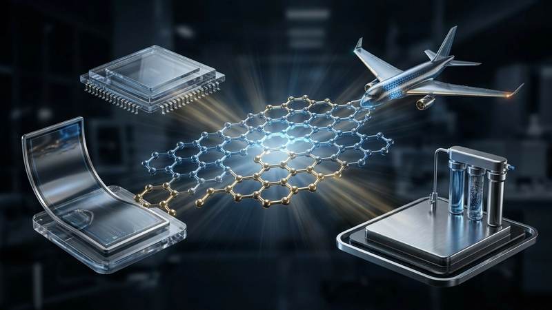
Future Horizons & High-Value B2B Applications
Graphene's intrinsic zero-bandgap and exceptionally high electron mobility, approaching 200,000 cm^2/Vs at room temperature, position it as a cornerstone for next-generation optoelectronic and high-frequency devices. Its ballistic transport properties enable superior performance in terahertz (THz) radiation detection and generation, promising breakthroughs in secure communication, medical imaging, and non-destructive testing, with prototypes demonstrating detection sensitivities in the picowatt range. The material's atomic thinness and mechanical flexibility are driving the development of truly bendable and stretchable electronics, from wearable health monitors to conformable RF antennas operating at gigahertz frequencies without degradation over thousands of flex cycles. Furthermore, the unique spin dynamics in graphene, characterized by long spin diffusion lengths (up to 100 µm at room temperature), are foundational for spintronic devices, potentially leading to ultra-low-power, non-volatile memory and neuromorphic computing architectures that mimic biological synapses, offering energy efficiencies orders of magnitude beyond conventional CMOS. The precise control over graphene's electronic structure through doping or strain engineering opens pathways for tunable bandgaps, addressing the critical need for semiconductor-like behavior in specific transistor designs, pushing operating frequencies and reducing power dissipation.
Beyond electronics, graphene's expansive surface area and tunable electronic structure are revolutionizing energy storage and environmental remediation. In electrochemical energy storage, functionalized graphene architectures have demonstrated specific capacitances exceeding 500 F/g in supercapacitors, enabling rapid charge-discharge cycles and superior power densities crucial for electric vehicles and grid-scale storage. For advanced battery technologies, graphene-enhanced anodes significantly improve lithium-ion intercalation kinetics, reducing charging times and extending cycle life, while also serving as robust hosts for next-generation solid-state electrolytes. In environmental applications, the material's unparalleled adsorptive capacity, driven by its high surface-to-volume ratio and specific surface chemistry, is being leveraged for water purification; graphene oxide membranes have shown heavy metal adsorption efficiencies of up to 79% for lead (Pb2+) and cadmium (Cd2+) ions in aqueous solutions within minutes. Furthermore, graphene-based photocatalysts, often hybridized with metal oxides like TiO2, exhibit enhanced quantum efficiencies for pollutant degradation and hydrogen production, utilizing a broader spectrum of solar energy through optimized charge separation and transfer mechanisms, with reaction times measurable in milliseconds.
The material's unparalleled mechanical strength, with a tensile strength of approximately 130 GPa and a Young's modulus of 1 TPa, coupled with its extraordinary thermal conductivity exceeding 5000 W/mK, renders it transformative for advanced composites and thermal management solutions. Integrating minute quantities of graphene into polymers, ceramics, and metals yields lightweight, high-performance materials for aerospace, automotive, and construction sectors, offering superior durability, fatigue resistance, and EMI shielding. For instance, graphene-enhanced composites are enabling aerospace structural components with a 30% weight reduction while maintaining or exceeding current performance standards. In thermal management, graphene films and foams are being developed for high-power electronics and data centers, capable of dissipating localized heat fluxes of several hundred W/cm^2, maintaining operational stability and extending device lifespans. Its biocompatibility and electrical conductivity are also driving innovation in the biomedical field, from ultra-sensitive biosensors capable of detecting biomarkers at picomolar concentrations to advanced neural interfaces and targeted drug delivery systems, where graphene's surface can be functionalized for specific molecular recognition and controlled release kinetics under external stimuli, such as localized 3000K thermal pulses for drug activation.
Evaluate Our Quality
Serious about B2B integration? Test our premium Pulsed Electrical Resistive Carbon Heating turbostratic graphene in your lab. 100g sample packs available now.