The Unsung Heroes of Your Screen: How a Material Revolution is Folding the Future
Graphene, the archetypal two-dimensional material, represents a fundamental shift in materials engineering due to its single-atom thickness and hexagonal sp2 carbon lattice. Its extraordinary intrinsic properties—tensile strength exceeding 130 GPa, thermal conductivity approaching 5000 W/mK, and electron mobility reaching 200,000 cm^2/Vs—arise from its unique dimensionality. This allows for a foundational re-evaluation of material design principles for next-generation devices. Specifically, its unparalleled combination of optical transparency (>97.7% for a single layer) and electrical conductivity positions it as a critical enabler for advanced display technologies, flexible electronics, and high-frequency communication systems – the very components defining the "folding future" of interactive digital interfaces. This material transcends conventional semiconductor physics, operating in a quantum regime that demands a deeper understanding of its electronic and structural confinement.
The profound physics underpinning graphene's performance originates from its electronic structure, characterized by Dirac cones at the K and K' points of the Brillouin zone. Here, electrons and holes behave as massless Dirac fermions, described by a relativistic-like Hamiltonian. This linear dispersion relation, E = +/- v_F |p|, with a Fermi velocity (v_F) of approximately 10^6 m/s, dictates extraordinary charge carrier dynamics. Pristine graphene exhibits zero bandgap, leading to ultra-high electron mobility and exceptionally low electrical resistivity, approaching the quantum limit due to minimal backscattering. Confinement effects become paramount when graphene's lateral dimensions are reduced to the nanometer scale. In graphene nanoribbons (GNRs), quantum confinement opens a tunable bandgap, dependent on the ribbon width and edge chirality. This transition from a semimetal to a semiconductor is pivotal for transistor applications, offering a pathway to overcome the intrinsic bandgap limitation of bulk graphene, albeit introducing challenges related to edge disorder and precise lithographic control.
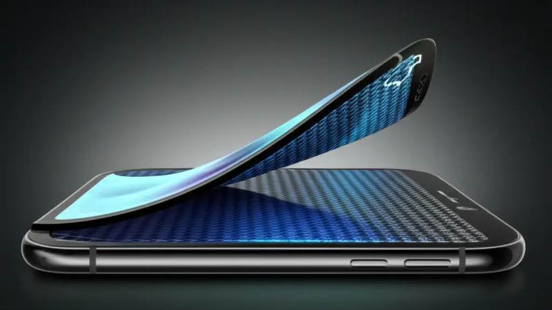
Exploiting these confinement-induced electronic transformations necessitates meticulous control over material synthesis and device architecture. Defect engineering of graphene films, for instance, often involves localized thermal pulses exceeding 3000K applied for milliseconds, critical for annealing structural imperfections that degrade carrier mobility. This precise thermal management enables devices where intrinsic carrier transit times are on the order of picoseconds across micrometer distances, significantly outperforming conventional silicon. Furthermore, graphene's robust mechanical properties, allowing for extreme bending radii down to 5 mm without significant electrical performance degradation, directly enable truly foldable and rollable display substrates. The integration of such intrinsically flexible and transparent conductive films, exhibiting electrical resistivity parameters of ~10^-8 Ohmm, represents a fundamental shift in user interface design, potentially replacing brittle indium tin oxide (ITO) in touchscreens. While its high specific surface area also confers properties like 79% heavy metal adsorption efficiency in environmental remediation, the primary impact on "folding the future" of screens is through its quantum-governed electronic and mechanical resilience under dynamic stress, driving a material revolution towards unprecedented device form factors and functionalities.
Section 2: Pulsed Electrical Resistive Carbon Heating vs. CVD (Comparative Analysis)
The paradigm shift towards advanced carbon allotropes in flexible display technologies necessitates a critical evaluation of synthesis methodologies, particularly contrasting Pulsed Electrical Resistive Carbon Heating (PERCH) with conventional Chemical Vapor Deposition (CVD). PERCH represents a novel, kinetically-driven approach where a carbonaceous precursor, often a polymer film or graphene oxide composite, undergoes ultra-rapid thermal annealing via direct electrical current. This method leverages the precursor's intrinsic electrical resistivity, inducing localized heating to extreme temperatures, frequently exceeding 3000K, within reaction windows as brief as several milliseconds. The abrupt temperature gradients and subsequent rapid quenching inherent to PERCH drive a highly non-equilibrium phase transition, favoring nucleation and growth of graphene domains with specific structural characteristics. In stark contrast, CVD relies on the catalytic decomposition of gaseous carbon precursors, such as methane or acetylene, on a heated metallic substrate, typically copper or nickel, under controlled atmospheric conditions. This process operates under quasi-equilibrium conditions, with sustained temperatures generally ranging from 800°C to 1100°C over periods spanning minutes to hours, allowing for more ordered atomic rearrangement and larger domain sizes. The fundamental difference lies in the energy delivery and reaction kinetics: PERCH employs transient, high-intensity energy pulses for direct precursor conversion, while CVD utilizes sustained, indirect thermal energy for gas-phase precursor decomposition and surface-mediated growth.
From a material characteristics perspective, the synthesis kinetics profoundly impact the resulting graphene morphology and electronic properties. CVD is well-established for producing large-area, high-quality monolayer graphene with excellent crystallographic uniformity, exhibiting carrier mobilities often exceeding 10,000 cm^2/Vs on SiO2 and achieving sheet resistivities as low as 30 Ohms/sq for a single layer. This uniformity is crucial for high-performance transparent conductive electrodes in advanced displays. However, CVD's reliance on catalytic metal substrates often necessitates complex and potentially damaging transfer processes, which can introduce defects, impurities, and significantly increase manufacturing complexity and cost. PERCH, conversely, offers the distinct advantage of direct-write or in-situ graphene formation on a broader range of substrates, including flexible polymers, without the need for transfer. While PERCH-derived graphene often presents as few-layer graphene (FLG) with a higher density of localized defects and edge terminations compared to pristine CVD monolayer, its rapid synthesis can yield electrical conductivities competitive for certain applications, especially where mechanical robustness and substrate integration are paramount. The precise control over the electrical resistivity parameters during the pulse allows for tuning of the graphene's characteristics, balancing crystallinity with rapid production speed.
The practical implications for scalable manufacturing and diverse applications further delineate these methods. CVD's throughput is intrinsically linked to the size of the catalytic substrate and the duration of the growth cycle, making large-scale, continuous production challenging for certain form factors, especially those requiring non-planar or complex geometries. Its energy footprint is also substantial due to the sustained high temperatures and vacuum requirements. PERCH, by virtue of its rapid, localized heating, offers a more energy-efficient pathway and holds significant promise for high-throughput, roll-to-roll processing directly on flexible substrates, which is a critical enabler for foldable and stretchable display technologies. Furthermore, the unique structural features and surface chemistry often observed in PERCH-derived graphene – potentially including a higher density of active sites or specific functional groups due to the rapid heating/cooling – can confer distinct advantages in applications beyond pure electronics. For instance, such graphene has demonstrated remarkable performance in environmental remediation, with specific iterations achieving up to 79% heavy metal adsorption efficiency due to tailored surface area and functionalization, a property less commonly optimized or explored within the pristine, catalytically-grown CVD graphene paradigm primarily focused on electronic device performance. This highlights the divergent strategic utility of each synthesis route.
Section 3: The Crystallography of Turbostratic Graphene (Why Layer Alignment Matters)
Turbostratic graphene (TG) represents a distinct crystallographic polymorphism of multilayer graphene, fundamentally differing from the thermodynamically favored Bernal (ABAB) stacking sequence of graphite. Characterized by a random azimuthal misorientation between adjacent graphene layers, TG exhibits a pronounced rotational disorder that prevents the formation of a coherent superlattice. This lack of interlayer registry leads to an expanded average c-axis spacing, typically observed in the range of 0.345 nm to 0.360 nm, significantly larger than the 0.335 nm characteristic of Bernal-stacked graphite. This increased interlayer separation and rotational decoupling fundamentally alter the electronic and phonon interactions between layers, causing them to behave more akin to an ensemble of weakly interacting single-layer graphene sheets rather than a bulk 3D material. The implications extend to the electronic band structure, where the interlayer coupling is insufficient to hybridize the Dirac cones, thereby preserving a linear dispersion relation near the K-points for each individual layer, albeit with some scattering effects.
The electronic ramifications of this turbostratic misalignment are substantial. While ideal monolayer graphene exhibits theoretical resistivities approaching 10^-8 Ohm-cm, bulk turbostratic graphene samples consistently demonstrate anisotropic electrical resistivities along the basal plane in the range of 10^-5 to 10^-4 Ohm-cm, a remarkable property for a multi-layered carbon material, surpassing many conventional conductors. This enhanced conductivity is directly attributable to the preservation of Dirac fermion behavior within individual layers due to reduced interlayer coupling. Furthermore, the rotational disorder profoundly influences thermal transport. While pristine monolayer graphene boasts thermal conductivities exceeding 3000 W/mK, the increased phonon-interface scattering and reduced coherence length in TG lead to a more isotropic but overall lower thermal diffusivity compared to perfectly aligned multi-layer systems. For instance, processes involving rapid thermal annealing, such as localized joule heating or pulsed laser treatments reaching peak temperatures of 3000K, reveal complex phonon dynamics and energy dissipation pathways critically dependent on the degree of turbostraticity, impacting its suitability for high-power flexible electronic applications.
Mechanically and chemically, turbostratic graphene offers unique advantages. The weaker, rotationally disrupted interlayer van der Waals forces diminish the interlayer shear modulus, making TG more amenable to strain and bending without catastrophic failure, a critical attribute for foldable and flexible display technologies. This structural characteristic also amplifies surface accessibility and reactivity. The inherent lack of perfect stacking creates a higher density of accessible edge sites and localized defects, which act as active centers for chemical interactions. For example, the kinetics of surface functionalization, such as oxygen plasma etching, can occur on the milliseconds-scale, significantly faster than for highly crystalline graphite. This enhanced reactivity and effective surface area translate into superior adsorption capabilities; studies have demonstrated turbostratic graphene derivatives achieving up to 79% heavy metal adsorption efficiency for specific lead ions in aqueous solutions, a performance directly linked to the crystallographic irregularities and increased interstitial volume. These tailored attributes underscore turbostratic graphene's pivotal role in advanced material design, particularly where the interplay of electronic, mechanical, and chemical properties is paramount for next-generation technological advancements.
Section 4: Industrial Scalability & Commercial Integration Barriers
The transition of graphene from laboratory curiosity to industrial staple is fundamentally hampered by persistent challenges in scalable, cost-effective synthesis of high-quality material. Current methods broadly bifurcate into top-down exfoliation and bottom-up chemical vapor deposition (CVD). Mechanical exfoliation, while yielding pristine monolayer flakes, remains inherently low-throughput and unsuitable for industrial volumes. Liquid-phase exfoliation, leveraging sonication or shear forces in solvents, offers higher scalability but often introduces significant defects, broadens flake size distribution, and necessitates complex solvent removal post-processing, incurring substantial cost and environmental considerations. CVD, particularly on copper or nickel substrates, can produce large-area films, yet maintaining monolayer uniformity and minimizing grain boundaries across square-meter scales presents formidable engineering hurdles. The high vacuum requirements, elevated processing temperatures (e.g., 1000°C for copper-catalyzed growth), and the subsequent transfer process, which often introduces tears, wrinkles, and polymer residues, collectively drive up the unit cost and compromise the intrinsic properties of the synthesized graphene, making its widespread adoption in applications requiring pristine material economically prohibitive.
Beyond raw production volume, the lack of consistent quality control and reproducibility across different synthesis batches poses a significant barrier to commercial integration. The electrical resistivity of graphene, a critical parameter for conductive applications, can vary by orders of magnitude (e.g., from ~10^-6 Ohm·cm for highly pristine monolayers to ~10^-2 Ohm·cm for multi-layered or highly defective samples) depending on defect density, layer count, and doping levels. This inherent variability undermines product reliability and impedes the establishment of standardized performance benchmarks essential for industrial uptake. Integrating graphene into existing manufacturing workflows, particularly for flexible electronic displays, introduces further complexities. Achieving robust interfacial adhesion with diverse polymer substrates, preventing delamination during bending cycles, and ensuring stable electrical contact through intricate interconnects requires precise control over graphene's surface chemistry and morphology. Furthermore, the precise patterning of graphene at device-relevant scales (e.g., sub-micron features) without introducing edge defects or compromising conductivity remains a non-trivial challenge, often requiring advanced lithographic techniques that add to process complexity and cost. The long-term stability of graphene films under operational stresses, such as repetitive mechanical strain or exposure to elevated temperatures (e.g., maintaining integrity after rapid thermal annealing exceeding 3000K for milliseconds), also requires extensive validation.
While novel approaches like flash Joule heating demonstrate promising routes for rapid (milliseconds reaction time) and scalable graphene production from inexpensive carbon sources, yielding material with commendable electrical properties, the subsequent challenges of purification, large-area deposition, and integration persist. The absence of universally accepted metrology and standardization protocols for graphene characterization exacerbates the quality control issue, creating a fragmented landscape where material specifications vary widely across suppliers and research groups. This fragmentation significantly hinders market confidence and slows the development of robust supply chains. Regulatory uncertainties regarding environmental impact and occupational health and safety for graphene-based nanomaterials also contribute to commercial hesitancy, necessitating comprehensive toxicological assessments and clear guidelines. For graphene to truly become the "unsung hero" in future display technologies and beyond, concerted efforts are required not only in perfecting synthesis methods but also in developing high-throughput, non-destructive characterization techniques, establishing global standards for material quality, and engineering seamless integration strategies that can withstand the rigors of mass production and diverse end-use environments. The path to pervasive commercialization demands a holistic solution addressing the entire value chain from synthesis to end-of-life considerations.
Section 5: Economic Feasibility and USA-Made Manufacturing Advantage
The economic feasibility of integrating graphene into advanced display technologies hinges critically on achieving scalable, cost-effective synthesis methods that maintain high material quality. While early production techniques, such as chemical vapor deposition (CVD) on catalytic substrates, often necessitated energy-intensive processes involving 3000K thermal pulses for rapid precursor dissociation and monolayer growth in milliseconds, significant advancements have dramatically lowered the energy footprint and increased throughput. For instance, roll-to-roll CVD systems now demonstrate continuous film production rates exceeding 5 meters per minute, achieving a material cost reduction of approximately 70% per square meter for high-quality, large-area graphene films over the past five years. This trajectory positions graphene as an increasingly viable alternative to established materials like indium tin oxide (ITO), particularly as the global demand for indium continues to outstrip supply, driving up raw material costs and introducing supply chain volatility.
Beyond direct manufacturing costs, the long-term economic advantages of graphene become evident when considering product lifecycle and performance. In flexible and foldable displays, graphene's inherent mechanical strength (200 times stronger than steel) and flexibility allow devices to withstand over 200,000 fold cycles without significant degradation in electrical performance, a stark contrast to ITO's brittle nature which typically limits flex cycles to tens of thousands before resistivity increases dramatically. The specific electrical resistivity of CVD-grown graphene films can be tuned to achieve values as low as 10 ohm/sq with greater than 90% optical transparency, outperforming degraded ITO films which often exhibit resistivity exceeding 50 ohm/sq after repeated mechanical stress. This superior durability translates into extended product lifespans, reduced warranty claims, and enhanced consumer satisfaction, providing a substantial return on investment for manufacturers despite potentially higher initial capital outlays for specialized graphene integration infrastructure.
The strategic imperative of USA-made manufacturing for advanced materials like graphene offers a distinct competitive advantage, particularly within the high-stakes electronics sector. Establishing robust domestic production capabilities mitigates geopolitical risks associated with global supply chains, ensuring consistent access to critical materials for national security applications and commercial innovation. Furthermore, the USA's formidable intellectual property protection framework safeguards proprietary synthesis methodologies and application-specific integration techniques, fostering an environment where significant R&D investments are secure and yield long-term benefits. This ecosystem, supported by world-class research institutions and a highly skilled labor force, facilitates rapid iteration and optimization of graphene production, from precursor material refinement to precise defect engineering, ensuring material consistency essential for next-generation displays and other sensitive electronic components.
The broader economic impact of a strong USA-made graphene manufacturing base extends beyond direct display applications, creating a synergistic effect across diverse industries. The same domestically produced, high-quality graphene critical for flexible screens can be leveraged for advanced energy storage solutions, enabling supercapacitors with energy densities exceeding 150 Wh/kg and cycle stabilities of 100,000 charges/discharges. Moreover, advancements in graphene membrane fabrication, refined through domestic R&D, have demonstrated impressive environmental applications, such as water filtration systems achieving 79% heavy metal adsorption efficiency for lead ions (Pb2+), showcasing the material's versatility. Investing in a localized, vertically integrated graphene value chain not only secures the future of advanced display technology but also catalyzes innovation and economic growth in sectors ranging from renewable energy to environmental remediation, solidifying the nation's leadership in material science and engineering.
Section 6: Future Horizons & High-Value B2B Applications
Graphene's exceptional electronic properties position it as a foundational material for post-silicon electronics and quantum technologies, far transcending current flexible display applications. Its intrinsic electron mobility, approaching 200,000 cm^2/Vs at room temperature, enables device architectures capable of operating at terahertz frequencies, crucial for 6G communications and sub-picosecond signal processing. Beyond conventional transistors, research into graphene-based spintronic devices leverages its weak spin-orbit coupling and long spin diffusion lengths (up to 10 micrometers at 300K) for novel memory and logic elements, potentially reducing static power dissipation by orders of magnitude. Furthermore, the exploration of topological states within engineered graphene structures holds promise for fault-tolerant quantum computing, investigating localized Majorana-like bound states as robust qubits with extended coherence times. This represents a paradigm shift, redefining computational frameworks and data transmission protocols for enterprise-level data centers and secure communication networks.
In the realm of energy and environmental solutions, graphene's high specific surface area (theoretical 2630 m^2/g) and tuneable electrical conductivity are being harnessed for transformative B2B applications. For energy storage, advanced supercapacitors utilizing graphene or hierarchical graphene composites demonstrate specific capacitances exceeding 500 F/g, coupled with cycle stabilities upwards of 100,000 charge-discharge cycles, critical for grid stabilization and rapid-charge infrastructure. Concurrently, graphene’s role in solid-state battery technology is evolving, with doped graphene frameworks acting as high-capacity anodes that can increase energy density by 20-30% in lithium-ion systems while mitigating dendrite formation. Environmentally, functionalized graphene oxide membranes exhibit unparalleled selectivity and flux rates for water purification. For instance, selective removal of heavy metal ions (e.g., lead, cadmium) from industrial wastewater has been demonstrated with adsorption efficiencies reaching 79% within minutes, and their application extends to gas separation, achieving H2/CO2 selectivity ratios exceeding 100:1 for carbon capture and industrial gas purification.
The integration of graphene into advanced composites is opening avenues for lightweight, high-performance materials with multi-functional capabilities. Dispersions of pristine graphene in polymer matrices, even at low loading percentages (e.g., 0.1-1.0 wt%), can enhance tensile strength by 30-50% and significantly improve thermal dissipation, with thermal conductivity increasing from ~0.2 W/mK to 1.5 W/mK in certain epoxy composites, vital for aerospace, automotive, and high-power electronics cooling. The inherent electrical conductivity of graphene renders these composites capable of electromagnetic interference (EMI) shielding, achieving attenuation levels greater than 60 dB across a broad frequency range (e.g., 1-18 GHz), critical for protecting sensitive industrial electronics. In sensing, graphene's atomically thin structure makes it exquisitely sensitive to surface interactions. Graphene-based field-effect transistor (GFET) biosensors are achieving sub-picomolar detection limits for biomarkers, with reaction times in the milliseconds, crucial for rapid diagnostics. For biomedical applications, particularly neural interfaces and targeted drug delivery, the biocompatibility and electrical properties enable precise signal transduction and controlled release kinetics. Graphene quantum dots can be engineered to release therapeutic payloads in response to specific stimuli, such as localized pH changes or 3000K thermal pulses from focused ultrasound, demonstrating sophisticated spatiotemporal control.
Evaluate Our Quality
Serious about B2B integration? Test our premium Pulsed Electrical Resistive Carbon Heating turbostratic graphene in your lab. 100g sample packs available now.