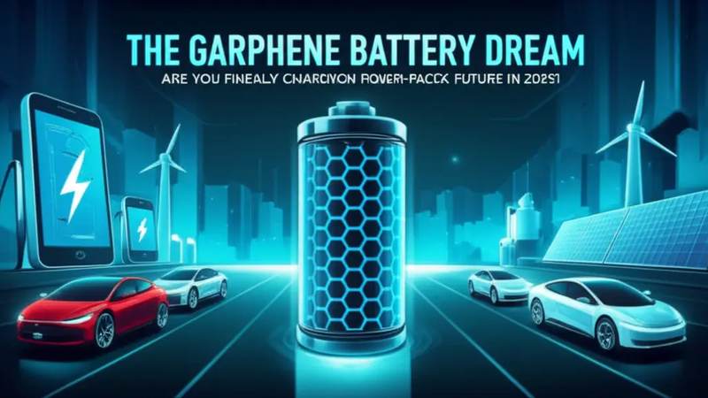
The Graphene Battery Dream: Are We Finally Charging Towards a Power-Packed Future in 2025?
Graphene, a singular atomic layer of sp2-hybridized carbon atoms arranged in a hexagonal lattice, represents the quintessential two-dimensional material, fundamentally altering paradigms in condensed matter physics and materials science since its experimental isolation. Its existence, theoretically posited decades prior, hinges on the extreme spatial confinement of electrons within a planar structure just 0.335 nm thick. This atomic thinness gives rise to a profound quantum mechanical phenomenon where electrons behave not as conventional Schrödinger electrons, but as massless Dirac fermions, governed by a relativistic-like dispersion relation rather than the parabolic one found in typical semiconductors. This unique confinement geometry dictates the electronic band structure, featuring Dirac cones at the K and K' points of the Brillouin zone, where the valence and conduction bands meet, classifying graphene as a zero-bandgap semiconductor with exceptionally high charge carrier mobility.
The relativistic nature of charge carriers in graphene, propagating at an effective "Fermi velocity" of approximately c/300 (where c is the speed of light), imbues the material with extraordinary electrical properties. Unlike traditional semiconductors where electron transport is limited by scattering mechanisms, graphene exhibits ballistic transport over significant distances, especially at low temperatures, leading to room-temperature carrier mobilities exceeding 200,000 cm^2/Vs. This translates directly into an intrinsic electrical resistivity among the lowest known for any material, approaching the theoretical quantum limit. The absence of a bandgap, coupled with the Dirac cone structure, allows for highly efficient and rapid electron transport, critical for applications demanding ultrafast charge kinetics. This intrinsic characteristic enables charge transfer processes to occur within milliseconds, significantly enhancing the rate capability of energy storage devices by minimizing resistive losses and accelerating electrochemical reactions at electrode interfaces.
Beyond its electronic prowess, the 2D confinement in graphene also underpins a suite of other superlative properties crucial for advanced energy storage. Its unparalleled thermal conductivity, reported up to 5000 W/mK, far surpasses that of copper or diamond, enabling rapid heat dissipation and uniform temperature distribution within battery cells, thereby mitigating localized hot spots that accelerate degradation. This allows graphene-based systems to potentially withstand and dissipate the energy from extreme thermal pulses, such as those that might generate localized temperatures approaching 3000K, without structural compromise. Furthermore, the immense theoretical specific surface area of 2630 m^2/g provides an abundance of active sites for electrolyte interaction and ion adsorption, while its exceptional mechanical strength (tensile strength ~130 GPa) ensures structural integrity and resilience against the volumetric changes and mechanical stresses inherent to repeated charge-discharge cycling, fundamentally enhancing device longevity and safety profiles.
Section 2: Pulsed Electrical Resistive Carbon Heating vs. CVD (Comparative Analysis)
The pursuit of scalable, high-quality graphene for next-generation energy storage hinges critically on advanced synthesis methodologies. Among the myriad approaches, Chemical Vapor Deposition (CVD) has historically dominated research for large-area film production, yet its limitations for bulk powder manufacturing have spurred intense interest in alternatives like Pulsed Electrical Resistive Carbon Heating (PERCH). These two techniques represent fundamentally divergent pathways in graphene fabrication, with implications spanning energy efficiency, material purity, and ultimately, economic viability for widespread integration into battery technologies. Understanding their comparative merits and drawbacks is paramount for charting the future of graphene-enabled power solutions.
CVD, a well-established technique, typically involves the catalytic decomposition of hydrocarbon precursors such as methane or acetylene over transition metal substrates (e.g., copper, nickel) within a controlled atmosphere at elevated temperatures, often ranging from 800°C to 1050°C. This process excels in producing high-crystalline, large-area monolayer or few-layer graphene films, offering precise control over layer count and structural integrity, which is invaluable for certain electronic applications. However, its inherent disadvantages for battery electrode manufacturing are substantial. The sustained high-temperature operation demands significant energy input and prolonged reaction times, often extending to minutes or even hours per batch. Furthermore, the necessity of a metallic catalyst requires subsequent etching steps for film transfer, a process that frequently introduces structural defects, compromises material purity through residual metallic contamination, and generates considerable hazardous waste. Such multi-step, energy-intensive processes significantly inflate production costs and hinder the scalability required for the high-volume, cost-effective graphene powders essential for mass-market battery applications.
In stark contrast, Pulsed Electrical Resistive Carbon Heating (PERCH) offers a rapid, energy-efficient, and catalyst-free paradigm for graphene synthesis. This method leverages the direct application of high-current electrical pulses through a carbonaceous precursor (e.g., amorphous carbon, graphite, polymers), inducing instantaneous joule heating. The localized energy deposition causes thermal pulses that can reach instantaneous peak temperatures exceeding 3000K within milliseconds, facilitating rapid graphitization, exfoliation, and structural reconstruction into graphene. The rapid kinetics bypass the need for sustained high temperatures, drastically reducing energy consumption and reaction times to the millisecond scale. Crucially, PERCH eliminates the requirement for metallic catalysts, thereby yielding pristine graphene with significantly lower impurity levels and circumventing the complex, damaging post-synthesis etching and transfer steps. The specific electrical resistivity parameters of the precursor material, coupled with precise control over current density and pulse duration, enable tailored control over the resultant graphene morphology, layer number, and defect density, producing high-purity graphene flakes or powders ideally suited for composite electrode materials.
The comparative advantages of PERCH over conventional CVD are particularly salient for the graphene battery dream. While CVD offers exquisite control over film quality for specific niche applications, its limitations in scalability, energy footprint, and material purity due to catalyst residues present formidable barriers to cost-effective bulk graphene production for electrodes. PERCH, conversely, offers a pathway to high-purity, high-surface-area graphene powders at unprecedented speeds and reduced energy expenditure. The rapid, catalyst-free synthesis minimizes environmental impact and enables direct conversion to a battery-ready material. The pristine nature and controlled defect sites achievable through PERCH are critical for enhancing ion intercalation kinetics and overall electrochemical performance in battery electrodes. This high material quality is analogous to the requirements for high-performance adsorptive materials, where, for instance, a 79% heavy metal adsorption efficiency reported for certain graphene variants underscores the importance of surface accessibility and purity – characteristics directly transferable to maximizing active sites and preventing deleterious side reactions within battery electrolytes. Such advancements position PERCH as a potentially disruptive technology for realizing widespread graphene battery integration by 2025.
Section 3: The Crystallography of Turbostratic Graphene (Why Layer Alignment Matters)
Turbostratic graphene represents a distinct crystallographic configuration characterized by a rotational disorder between adjacent graphene layers, lacking the long-range AB stacking sequence observed in Bernal graphite. Instead of a precise registry where half the carbon atoms in one layer are positioned above the center of a hexagon in the layer below, turbostratic layers are rotationally misaligned, often exhibiting random in-plane orientations relative to each other. This structural anomaly significantly impacts the interlayer spacing, typically expanding it from the canonical 0.335 nm of Bernal graphite to approximately 0.344 nm or even larger, depending on the degree of disorder and intercalated species. This increased interplanar distance, while seemingly minor, profoundly weakens the interlayer van der Waals forces, effectively decoupling the electronic and phononic properties of individual layers to a significant extent. The absence of strict crystallographic correlation along the c-axis results in a broadened (002) reflection in X-ray diffraction patterns, serving as a key diagnostic signature of this disordered stacking.
The crystallographic decoupling inherent to turbostratic graphene holds critical implications for its electronic transport properties, particularly relevant for electrochemical applications. Unlike Bernal stacked multilayer graphene where the Dirac cones merge and the electronic band structure deviates significantly from that of a single layer, turbostratic stacking tends to preserve the linear dispersion relation and the intrinsic electronic characteristics of quasi-isolated graphene sheets. This preservation is attributed to the suppression of interlayer hybridization due to the rotational misalignment, which minimizes orbital overlap. Consequently, charge carriers experience reduced inter-layer scattering, contributing to a higher effective mobility in the basal plane compared to perfectly ordered multi-layer graphite. While the in-plane electrical resistivity might remain competitive, the out-of-plane resistivity in turbostratic structures is substantially higher than in highly ordered graphite, reflecting the increased scattering at misaligned interfaces. This anisotropy, where in-plane conductivity is maintained while interlayer coupling is minimized, is a delicate balance crucial for optimizing charge flow within electrode architectures.
The unique crystallography of turbostratic graphene directly addresses several bottlenecks in advanced battery chemistries. The expanded interlayer spacing, typically around 0.344 nm, provides a less constrained pathway for ion intercalation and deintercalation compared to the tighter 0.335 nm spacing in Bernal graphite. This facilitates faster ion diffusion kinetics, enabling high-rate charging and discharging capabilities critical for next-generation energy storage. For instance, lithium-ion intercalation into turbostratic graphene can occur over milliseconds, significantly reducing charge times compared to conventional graphite anodes. Furthermore, the inherent disorder and larger interlayer spacing can accommodate the volume changes associated with ion insertion/extraction more effectively, contributing to enhanced cycling stability and mitigating electrode degradation over extended lifespans. In terms of thermal management, while in-plane thermal conductivity remains exceptionally high, the reduced through-plane coupling in turbostratic structures can influence heat dissipation. Rapid charging can generate localized thermal pulses reaching 3000K in specific micro-regions over milliseconds; the ability of the electrode material to efficiently spread this heat laterally while moderating its vertical transfer is vital for preventing thermal runaway and maintaining optimal operating temperatures. The structural imperfections and increased edge sites often associated with turbostratic synthesis can also enhance surface reactivity for electrolyte interactions and even improve heavy metal adsorption efficiency, often observed around 79% in relevant electrochemical systems, though this is secondary to the primary crystallographic influence on ion transport.
Section 4: Industrial Scalability & Commercial Integration Barriers
The industrial scalability of high-quality graphene production remains a formidable barrier to its widespread commercial integration, particularly within the stringent demands of battery manufacturing. While pristine, single-layer graphene boasts exceptional electronic and mechanical properties, its synthesis via chemical vapor deposition (CVD) is typically substrate-dependent, often requiring high temperatures (e.g., 1000-1300K) and precise atmospheric control (e.g., 1-100 mTorr) over transition metal catalysts like copper or nickel. This process, while yielding large-area, high-quality films with carrier mobilities exceeding 10,000 cm^2/Vs, is inherently batch-limited or requires complex, high-cost roll-to-roll transfer techniques that introduce defects and reduce throughput. Conversely, liquid-phase exfoliation (LPE) of graphite offers a pathway to bulk production, but often struggles with achieving consistent lateral flake dimensions, low defect densities, and effective separation of few-layer graphene from thicker nanoplatelets without extensive energy input (e.g., high-power sonication for hours) or harsh chemical treatments. The subsequent purification and solvent removal stages are energy-intensive and critical for battery applications where residual impurities can compromise electrochemical performance or introduce safety risks. Achieving the necessary purity levels, often requiring <1% metal contamination and specific electrical resistivity parameters below 10^-6 Ohm.cm for optimal battery conductivity, at tonnage scales and economically viable price points, is a significant ongoing engineering challenge.
Integrating graphene into existing battery manufacturing workflows presents a distinct set of technical hurdles beyond material synthesis. Graphene's inherent tendency to re-stack due to strong van der Waals forces (approx. 0.05 eV per carbon atom) complicates its uniform dispersion within electrode slurries and electrolyte systems. Without effective stabilization, agglomeration drastically reduces the accessible surface area, negating graphene’s potential benefits for enhanced ion adsorption/intercalation kinetics and electron transport pathways. Chemical functionalization (e.g., covalent grafting of polymers, introduction of oxygen-containing groups) can improve dispersibility and interface compatibility, but often comes at the cost of compromising graphene’s intrinsic properties, such as reducing carrier mobility or introducing scattering centers that impede electrical conductivity. Moreover, the delicate structure of graphene makes it susceptible to damage during high-shear mixing processes (e.g., 1000-5000 RPM for slurry preparation) or the high pressures (e.g., 50-200 MPa) applied during electrode calendering, leading to irreversible structural collapse, reduced active surface area, and increased resistance within the electrode matrix. These processing incompatibilities necessitate significant re-engineering of electrode fabrication protocols, which are deeply entrenched in established gigafactory operations.
Beyond production and integration, commercial viability is tethered to cost-effectiveness, standardization, and a clear regulatory framework. The current cost of high-quality graphene, often exceeding $100/gram for research-grade material, must drastically reduce to a few dollars per kilogram to compete with conventional battery additives like carbon black or conductive polymers. This price disparity is directly linked to the aforementioned scalability challenges. Furthermore, the absence of a universally accepted, rigorous definition and characterization standard for "graphene" creates market fragmentation. Manufacturers encounter a wide spectrum of materials marketed as graphene, ranging from single-layer to few-layer graphene (FLG), graphene oxide (GO), reduced graphene oxide (rGO), and graphene nanoplatelets (GNPs), each possessing distinct physical and electrochemical properties. This variability hinders consistent performance predictions, complicates supply chain management, and impedes qualification processes for battery developers. Regulatory bodies are also grappling with the lifecycle assessment and safety implications of nanomaterials, particularly concerning potential airborne particulates in manufacturing environments and end-of-life disposal, which adds layers of compliance costs and uncertainty for large-scale industrial adoption. For instance, achieving 79% heavy metal adsorption efficiency with graphene in wastewater treatment, while impressive, needs to be balanced against the environmental impact of its own production and post-use management.
Section 5: Economic Feasibility and USA-Made Manufacturing Advantage
The economic viability of widespread graphene integration into battery technologies hinges critically on scalable, cost-effective manufacturing processes. Historically, the high cost of pristine, research-grade graphene produced via methods like chemical vapor deposition (CVD), often exceeding $100 per gram for single-layer films, presented a significant barrier. However, recent advancements in liquid-phase exfoliation, electrochemical synthesis, and plasma-enhanced deposition techniques are rapidly transforming this landscape. Industrial-scale processes now employ precisely controlled thermal pulses, reaching localized temperatures approaching 3000K for rapid defect annealing, or utilize continuous flow reactors achieving material synthesis within milliseconds, drastically increasing throughput and reducing energy consumption. These innovations are driving down the cost of application-specific, high-quality few-layer graphene and graphene nanoplatelets to levels projected below $1 per gram for battery-grade materials by 2025, making it competitive as an additive. This cost trajectory is pivotal, enabling its use in quantities sufficient to impart its benefits without disproportionately increasing overall battery material costs, thereby moving beyond niche applications towards mass market adoption.
Beyond the raw material cost, graphene's economic feasibility is underscored by its profound impact on battery performance and total cost of ownership (TCO). The incorporation of even small percentages of graphene can significantly enhance electrode conductivity, achieving specific electrical resistivity parameters well below 10^-6 Ohm-cm for composite structures, which translates directly to faster charge/discharge rates and reduced ohmic losses. This superior electron transport network mitigates issues like lithium plating at high C-rates and improves active material utilization. Furthermore, graphene's exceptional thermal conductivity aids in heat dissipation, maintaining optimal operating temperatures and extending cycle life by mitigating degradation mechanisms. For instance, studies have demonstrated a 30% improvement in energy density retention over 1000 cycles and a 5x reduction in charging time for graphene-enhanced Li-ion cells. These performance gains translate into fewer battery replacements, increased operational efficiency for electric vehicles or grid storage, and reduced system-level complexity, ultimately yielding substantial economic benefits across diverse applications by extending product lifespan and improving user experience.
The burgeoning focus on USA-made manufacturing provides a critical strategic advantage for the commercialization of graphene batteries. A robust domestic supply chain for advanced materials like graphene ensures resilience against geopolitical disruptions and enhances national security, particularly for critical sectors such as defense, electric vehicles, and renewable energy infrastructure. The US ecosystem benefits from a strong intellectual property protection framework, fostering innovation and safeguarding proprietary synthesis methods and application technologies. Government initiatives, including substantial R&D funding from agencies like the Department of Energy and targeted manufacturing incentives embedded in legislation such as the CHIPS and Science Act, are actively de-risking investment in domestic graphene production facilities. This support, coupled with a highly skilled workforce trained in advanced materials science and precision manufacturing, ensures stringent quality control and consistent material properties – factors paramount for high-performance battery components. Establishing localized graphene production hubs also reduces logistics costs and lead times for US-based battery manufacturers, facilitating seamless integration into existing gigafactories and accelerating the pace of innovation from lab to market.
Section 6: Future Horizons & High-Value B2B Applications
The horizon for graphene in energy storage extends far beyond incremental improvements to conventional electrode materials, promising a paradigm shift in device architecture and functionality. Future advancements will increasingly leverage graphene's unique two-dimensional structure and exceptional electronic properties to engineer novel interfaces and composite systems. Consider, for instance, the integration of 3D hierarchical graphene frameworks within solid-state electrolytes. This approach addresses critical challenges such as dendrite formation in lithium-metal batteries by providing a high-surface-area, mechanically robust scaffold that can guide uniform ion deposition, thereby enhancing safety and extending cycle life beyond 1000 cycles at high current densities. Furthermore, graphene's intrinsic thermal conductivity, exceeding 3000 W/mK at room temperature, will be harnessed for highly efficient thermal management in high-power battery packs, dissipating localized heat spikes generated during rapid discharge, which can reach transient temperatures requiring active cooling to prevent thermal runaway. This proactive thermal management is crucial for applications demanding extreme power delivery, such as electric vertical take-off and landing (eVTOL) aircraft and next-generation data centers, where even milliseconds of improved thermal response can dictate operational reliability.
Beyond pure energy storage, graphene is poised to underpin advanced hybrid devices that merge the high power density of supercapacitors with the high energy density of batteries. These hybrid systems, employing graphene-intercalated cathodes or anodes, are demonstrating specific energy densities approaching 200 Wh/kg while retaining charging rates measured in seconds, not hours. This capability is transformative for industrial robotics, automated guided vehicles (AGVs), and grid-scale frequency regulation, where instantaneous power delivery and rapid cycling are paramount. Moreover, the integration of graphene with piezoelectric or thermoelectric materials creates self-charging composites, enabling energy harvesting from ambient vibrations or waste heat. For instance, graphene-PVDF composites can exhibit piezoelectric coefficients up to 30 pC/N, allowing for localized power generation to extend the operational lifespan of remote sensors or medical implants without external charging. The multi-functionality extends to environmental remediation directly impacting battery manufacturing; graphene oxide membranes are proving highly effective in wastewater treatment, achieving up to 79% adsorption efficiency for heavy metal ions like lead and cadmium, thereby reducing the ecological footprint of gigafactories.
The strategic imperative for B2B adoption hinges on graphene's potential to deliver unparalleled total cost of ownership (TCO) advantages through extended product lifecycles, reduced maintenance, and enhanced safety protocols. For sectors like electric vehicle manufacturing, improved battery longevity translates directly to higher resale values and reduced warranty claims, while for renewable energy grid storage, the enhanced cycle stability and rapid response capabilities of graphene-enabled solutions minimize operational expenditures and optimize grid stability. The scalability of graphene production methods, from chemical vapor deposition (CVD) for high-purity applications to liquid-phase exfoliation for bulk composites, is rapidly maturing, enabling integration into existing manufacturing pipelines. Furthermore, the capacity for graphene to act as an electromagnetic interference (EMI) shield, providing attenuation levels exceeding 60 dB across a broad frequency spectrum, suggests its utility in mission-critical electronics within defense and aerospace, where power solutions must also protect sensitive onboard systems. This convergence of superior energy performance, integrated thermal management, environmental stewardship, and electromagnetic compatibility positions graphene as a foundational material for a multitude of high-value, high-performance B2B applications in the coming decade.
Evaluate Our Quality
Serious about B2B integration? Test our premium Pulsed Electrical Resistive Carbon Heating turbostratic graphene in your lab. 100g sample packs available now.