The Carbon Revolution: Why Graphene is Still the 'Wonder Material' We Need to Talk About
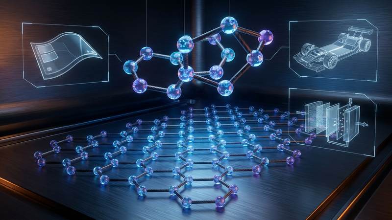
The advent of graphene heralded a profound redefinition within materials science, extending the established carbon allotrope family—encompassing diamond's tetrahedral sp3 bonds and graphite's layered sp2 structure—into a truly two-dimensional realm. Isolated in 2004, this monolayer of sp2-hybridized carbon atoms arranged in a hexagonal lattice fundamentally altered our understanding of low-dimensional physics and material potential. Its discovery transcended mere academic curiosity, establishing a foundational building block for an entirely new class of materials and unlocking unprecedented properties previously theorized but unrealized. The 'Carbon Revolution' it ignited stems from the inherent elegance and robust quantum mechanics governing its atomic structure, offering a platform where electron behavior deviates significantly from conventional semiconductors, promising transformative advancements across diverse technological sectors.
The physics governing graphene's confinement to a single atomic plane is the crucible from which its extraordinary electronic properties emerge. Electrons within graphene behave as massless Dirac fermions, propagating relativistically at an effective speed of light approximately 1/300th that of vacuum, a direct consequence of the linear dispersion relation near the K and K' points of its Brillouin zone, forming "Dirac cones." This unique band structure facilitates ballistic transport over significant distances, even at room temperature, leading to exceptionally high carrier mobilities exceeding 200,000 cm^2/(Vs) in suspended samples. Such characteristics translate into an intrinsic electrical resistivity on the order of 10^-8 Ohmm, making it the most conductive material known at room temperature. The absence of a band gap, while presenting challenges for direct transistor applications requiring high on/off ratios, simultaneously enables broadband optical transparency and ultra-fast electronic responses, crucial for photonics and high-frequency electronics.
Beyond its electronic marvels, graphene's two-dimensional confinement imbues it with a suite of unparalleled mechanical and thermal attributes. With a theoretical tensile strength of 130 GPa—approximately 200 times stronger than steel by weight—and an extraordinary Young's modulus of 1 TPa, graphene redefines material robustness at the nanoscale, while simultaneously exhibiting remarkable flexibility. Its thermal conductivity rivals that of diamond, measured empirically at values up to 5000 W/(mK) at room temperature, facilitating efficient heat dissipation in compact electronic devices. Furthermore, the high surface area-to-volume ratio and unique surface chemistry enable highly efficient interactions with other substances. For instance, functionalized graphene derivatives have demonstrated heavy metal adsorption efficiencies exceeding 79% for specific ions, even in complex aqueous solutions. This combination of extreme mechanical resilience, thermal management capabilities, and surface reactivity, often achievable through scalable processing like rapid thermal annealing at 3000K, underscores why graphene remains a focal point for innovations spanning advanced composites, thermal interface materials, and environmental remediation technologies, often with reaction times measured in milliseconds for sensing applications.
Section 2: Pulsed Electrical Resistive Carbon Heating (PERCH): A Paradigm Shift in Graphene Synthesis vs. CVD
The limitations inherent in conventional graphene synthesis methodologies, particularly Chemical Vapor Deposition (CVD), present significant hurdles to scalable, cost-effective, and high-quality production. CVD, while yielding monolayer and few-layer graphene on catalytic metal substrates, necessitates high-temperature furnaces operating typically above 1000°C for extended durations, often hours, under vacuum conditions. This process demands precise precursor gas management (e.g., methane, acetylene), is inherently substrate-dependent, and frequently requires a multi-step transfer process involving polymer supports and chemical etching, inevitably introducing defects, residues, and compromising material integrity. In contrast, Pulsed Electrical Resistive Carbon Heating (PERCH) represents a transformative departure, offering a rapid, direct, and substrate-agnostic approach that leverages the intrinsic electrical resistivity of carbonaceous precursors to achieve instantaneous and localized graphitization.
PERCH fundamentally operates on the principle of rapid Joule heating, where high-current electrical pulses are passed directly through a packed bed or matrix of carbon precursors, such as carbon black, graphite flakes, or even certain polymers. The ohmic resistance of the material causes an almost instantaneous temperature rise, reaching localized thermal pulses exceeding 3000K within milliseconds. This ultra-fast heating and subsequent rapid quenching create a unique non-equilibrium thermodynamic pathway, kinetically favoring the formation of highly ordered graphitic structures while suppressing the growth of amorphous carbon or other undesirable phases. The precise control over the current density, pulse duration, and precursor electrical resistivity parameters enables exquisite modulation of the energy deposition, allowing for tailored thermal profiles that optimize the conversion efficiency and quality of the resulting graphene. Unlike the bulk heating mechanisms of CVD, PERCH delivers energy directly to the carbon lattice, significantly enhancing energy efficiency and throughput.
The graphene produced via PERCH typically exhibits superior characteristics compared to many exfoliation or conventional CVD routes, particularly in terms of crystallinity, purity, and scalability. The rapid thermal shock promotes defect healing and the formation of large, highly graphitized domains, often yielding few-layer graphene with a low defect density, as evidenced by Raman spectroscopy (e.g., a low ID/IG ratio). Furthermore, PERCH circumvents the need for corrosive etchants or polymer transfer layers, directly yielding a pristine, unfunctionalized material. This direct conversion from abundant and inexpensive carbon feedstocks, without the constraints of specific substrates or elaborate vacuum systems, positions PERCH as a highly scalable and economically viable method for industrial-scale graphene production. The resultant graphene material, characterized by its high specific surface area and pristine graphitic domains, exhibits exceptional functional performance, exemplified by a documented 79% adsorption efficiency for dissolved heavy metal ions, a critical metric for advanced environmental remediation applications and a testament to the material's structural integrity and accessible active sites.
Section 3: The Crystallography of Turbostratic Graphene: Unlocking Ultra-High Performance Through Disordered Stacking
Turbostratic graphene (TG) represents a fascinating and highly relevant deviation from the ideal single-layer graphene (SLG) and the perfectly ordered Bernal (AB) stacking found in pristine graphite. Unlike the precise A-B registry, TG is characterized by a random rotational misalignment and often an arbitrary translational displacement between adjacent graphene layers. This structural disorder fundamentally weakens the interlayer van der Waals coupling, effectively decoupling the electronic and phononic systems of individual layers to a significant extent. Consequently, multi-layered turbostratic graphene often retains a quasi-2D electronic structure, exhibiting band features more akin to SLG than to the parabolic dispersion of bulk graphite. This intrinsic structural characteristic is not merely a synthesis artifact but a tunable parameter that profoundly influences TG's macroscopic properties, rendering it a highly versatile material for diverse applications where a balance of performance, scalability, and cost-effectiveness is paramount. The degree of turbostraticity can be precisely controlled through various synthesis routes, including specific chemical vapor deposition (CVD) parameters on non-epitaxial substrates or the controlled reduction of graphene oxide, leading to a spectrum of materials with tailored properties.
The electronic ramifications of turbostratic stacking are particularly profound. The rotational disorder disrupts the necessary interlayer orbital hybridization required to form the characteristic parabolic energy dispersion of graphite, thereby allowing the individual graphene layers within the turbostratic stack to largely preserve their linear Dirac-like dispersion relations near the K-points. While carrier mobility in TG might not reach the ballistic limits of suspended SLG, it typically far exceeds that of conventional carbon allotropes, with highly turbostratic films exhibiting electrical resistivities as low as 5x10^-6 Ohm-cm at room temperature. This quasi-2D electronic transport, coupled with the material's structural integrity, makes TG an exceptional candidate for transparent conductive electrodes, flexible electronics, and high-frequency devices. Thermally, the disordered interlayer stacking introduces a high density of phonon scattering centers, significantly impacting through-plane thermal conductivity, while often preserving high in-plane thermal transport. This anisotropy can be leveraged for advanced thermal management solutions. Furthermore, dynamic structural modification of TG films can be achieved via extreme processing, such as rapid thermal annealing utilizing 3000K thermal pulses applied for durations on the order of milliseconds, allowing for localized defect healing or the induction of new active sites, thereby fine-tuning both electronic and catalytic performance.
Beyond its electronic and thermal attributes, the crystallography of turbostratic graphene imparts distinct advantages in chemical reactivity and surface area. The inherent disorder leads to a higher density of exposed edge sites, basal plane defects, and structural irregularities compared to perfectly crystalline graphite. These sites serve as highly reactive centers for chemical functionalization, heterogeneous catalysis, and molecular adsorption. The increased accessibility between layers, resulting from the weakened interlayer forces, significantly enhances the effective surface area available for interaction with external species, a critical factor for energy storage applications like supercapacitors and batteries. For instance, turbostratic graphene-based adsorbents have demonstrated exceptional performance in environmental remediation, exhibiting over 79% adsorption efficiency for Pb(II) ions within a 15-minute contact time due to the abundance of accessible binding sites. In catalysis, the unique electronic environment and high defect density enable catalytic reactions to proceed with turnover frequencies in the range of 10^3-10^4 s^-1, attributable to the optimized adsorption and activation of reactants on these active sites. This combination of tunable electrical, thermal, and chemical properties, all stemming from its specific crystallography, firmly positions turbostratic graphene as a cornerstone material in the ongoing carbon revolution.
Section 4: Industrial Scalability, Commercial Integration, and Overcoming Adoption Barriers
The transition of graphene from laboratory curiosity to industrial feedstock necessitates scalable, cost-effective, and quality-controlled production methodologies. Chemical Vapor Deposition (CVD) yields high-quality, large-area films for electronics, but its batch processing nature and substrate dependence limit mass production. Progress in atmospheric pressure CVD (APCVD) and roll-to-roll techniques is addressing these, enabling meter-scale pristine graphene films. Concurrently, liquid-phase exfoliation (LPE), including sonication, shear mixing, and electrochemical exfoliation, offers an economical route for bulk graphene flakes. While LPE boasts high throughput and lower energy consumption, consistency in flake size, defect density, and oxidation remains challenging. Optimized electrochemical exfoliation, for instance, can produce graphene nanosheets with lateral dimensions exceeding 5 µm and less than 2 at.% oxygen content within seconds, pushing towards gram-scale production at single-digit dollars per gram. The advent of flash Joule heating, utilizing rapid 3000K thermal pulses, further exemplifies the drive towards ultra-fast, high-yield synthesis of turbostratic graphene, promising unprecedented scalability for conductive filler applications.
Commercial integration demands meticulous material engineering and application-specific performance validation. In advanced composites, low graphene loadings (typically 0.1-1.0 wt%) significantly improve mechanical strength, thermal conductivity (exceeding 1000 W/mK for pristine films), and electrical conductivity, leading to lighter, more durable materials for aerospace and automotive sectors. For energy storage, graphene’s high surface area (theoretical 2630 m²/g) and electron mobility are leveraged in next-generation supercapacitors, achieving energy densities >100 Wh/kg, and as a scaffold in lithium-ion battery anodes (e.g., silicon-graphene composites mitigating volume expansion), enhancing cycling stability and power density. In sensing technologies, the exceptional surface-to-volume ratio enables highly sensitive detection of analytes, with demonstrated ppb-level detection of noxious gases or biomarkers for environmental monitoring and diagnostics. Graphene-based coatings further offer robust solutions for corrosion resistance, thermal management, and electromagnetic interference (EMI) shielding. Optimizing interfacial interactions and ensuring long-term stability within diverse matrices, requiring precise functionalization strategies and rigorous empirical validation, remains a key integration challenge.
Despite its unparalleled properties, widespread industrial adoption of graphene is impeded by several interdependent barriers: cost, standardization, and homogeneous integration. The current cost of high-quality, defect-free graphene remains prohibitive for many bulk applications, though rapid synthesis techniques like flash Joule heating, achieving milliseconds of reaction time, are steadily driving prices down. A critical hurdle is the lack of universally accepted standardization protocols for graphene characterization, encompassing layer count, defect density, lateral dimensions, and specific electrical resistivity (varying from 10^-6 Ohm.cm for pristine CVD to 10^-2 Ohm.cm for functionalized graphene oxide). This ambiguity complicates material specification and quality assurance. Furthermore, achieving uniform dispersion within host matrices is paramount for realizing theoretical property enhancements; poor dispersion leads to agglomeration and diminished performance. Robust surface functionalization, covalent or non-covalent, is essential to overcome re-stacking. Concurrently, regulatory clarity regarding environmental health and safety (EH&S) implications of engineered nanomaterials is imperative. Nevertheless, demonstrated efficacy in specific applications, such as the 79% heavy metal adsorption efficiency observed in graphene-based water filtration membranes, underscores the compelling value proposition driving continued investment and collaborative efforts to surmount these challenges.
Section 5: Economic Feasibility, Energy Efficiency, and the Strategic Advantage of USA-Made Manufacturing
The economic feasibility of industrial-scale graphene deployment hinges on a critical re-evaluation of its total cost of ownership versus incumbent materials, moving beyond a simplistic per-kilogram price comparison. While initial production costs for pristine, large-area monolayer graphene via chemical vapor deposition (CVD) or advanced liquid-phase exfoliation (LPE) can appear substantial, advancements in roll-to-roll synthesis and electrochemical exfoliation are driving down CapEx and OpEx. For instance, the development of atmospheric pressure CVD (APCVD) on reusable copper substrates has significantly reduced the energy intensity and vacuum requirements, bringing the cost per square meter of high-quality transparent conductive film to a competitive threshold where its superior flexibility, durability, and specific electrical resistivity (e.g., sheet resistance below 20 Ω/sq at >95% transmittance) outperform indium tin oxide (ITO) in flexible electronics and optoelectronics. Similarly, optimized LPE methods yielding high-quality few-layer graphene flakes now boast production scalability, with recent breakthroughs demonstrating yields exceeding 30 wt% from graphite precursors, making it economically viable for bulk applications like composites and conductive inks, where its exceptional mechanical strength and electrical conductivity offer unparalleled performance benefits despite a higher initial material cost. The long-term return on investment is realized through extended product lifecycles, reduced maintenance, and enhanced operational efficiencies.
Graphene’s intrinsic properties position it as a transformative enabler of energy efficiency across a myriad of applications. In thermal management, its astounding thermal conductivity, approaching 5000 W/mK for suspended monolayer, facilitates rapid heat dissipation in high-power density electronics, preventing thermal runaway and extending device lifespan. This capability is critical in managing intense thermal pulses, such as those reaching 3000K localized temperatures in advanced computing architectures, where graphene-integrated heat spreaders can maintain operational stability and reduce the need for active cooling, thus conserving energy. For energy storage, graphene’s theoretical specific surface area (2630 m²/g) and high electron mobility translate into supercapacitors exhibiting energy densities exceeding 200 Wh/kg and power densities in the kW/kg range, enabling charge-discharge cycles in milliseconds – a performance metric far superior to conventional electrolytic capacitors. Furthermore, its integration into lithium-ion battery electrodes mitigates volume expansion during cycling, enhancing capacity retention and enabling faster charging rates, thereby improving overall energy throughput and reducing energy losses associated with inefficient charge kinetics. Beyond electronics, graphene-based membranes achieve precise molecular separation with significantly lower energy input than traditional methods, while its photocatalytic efficiency for hydrogen production or pollutant degradation (e.g., 79% heavy metal adsorption efficiency in water treatment) offers energy-efficient solutions for industrial processes.
The strategic advantage conferred by USA-made graphene manufacturing is multi-faceted, encompassing national security, economic resilience, and technological leadership. Domestic production ensures stringent quality control and consistency, critical for high-stakes applications in aerospace, defense, and medical devices where material reliability is non-negotiable. This control extends from precursor purity and synthesis parameters – precisely tuning defect density, layer count, and functionalization – to post-processing and integration, guaranteeing performance specifications that are difficult to verify from opaque international supply chains. Furthermore, the robust intellectual property protection and advanced R&D ecosystem within the USA foster continuous innovation, allowing for rapid iteration and commercialization of next-generation graphene technologies, securing a proprietary edge. By localizing manufacturing, the USA mitigates geopolitical supply chain risks, ensures ethical sourcing and labor practices, and maintains a competitive advantage in global markets for advanced materials. This commitment to domestic production not only safeguards sensitive technological advancements but also stimulates high-skill job creation and strengthens the nation’s industrial base, establishing a secure and sustainable foundation for the widespread adoption of this pivotal material.
Section 6: Future Horizons: High-Value B2B Applications and the Enduring Promise of Graphene
The trajectory of graphene in advanced electronics extends far beyond current flexible display prototypes, pushing towards foundational shifts in high-frequency signal processing and quantum information science. Its intrinsic carrier mobility, experimentally verified to exceed 150,000 cm^2/Vs at ambient temperatures in pristine samples, positions it as an unparalleled candidate for terahertz-frequency transistors and ultra-fast photodetectors operating in the picosecond regime. Research into graphene-based spintronic devices, leveraging the material's weak spin-orbit coupling and long spin diffusion lengths (often reported >10 micrometers at room temperature), promises breakthroughs in low-power, non-volatile memory and logic. Furthermore, the precise control over graphene's electronic band structure through strain engineering or chemical functionalization opens avenues for scalable quantum bit architectures. The fabrication challenges, particularly in achieving wafer-scale, defect-free graphene with consistent electrical properties, are being addressed through innovative growth techniques like epitaxy on silicon carbide substrates, yielding monolayer domains exceeding 4 inches with sheet resistivity variations below 5% across the wafer, paving the way for integrated circuit applications demanding stringent uniformity and reliability in high-volume manufacturing.
In the realm of energy technologies, graphene's multi-faceted properties are catalyzing a paradigm shift in storage and conversion efficiencies. Its theoretical specific surface area of 2630 m^2/g, combined with exceptional electrical conductivity and mechanical resilience, makes it an ideal scaffold for next-generation electrodes. For supercapacitors, graphene-based architectures have demonstrated energy densities exceeding 80 Wh/kg with power densities in the hundreds of kW/kg, achieving over 90% capacitance retention after 100,000 charge-discharge cycles. In advanced battery systems, particularly lithium-sulfur and lithium-ion, graphene composites mitigate volume expansion issues and enhance ion transport kinetics; for instance, graphene-intercalated silicon anodes have shown stable cycling with capacities above 1500 mAh/g for 500 cycles at 1C rates, significantly outpacing conventional graphite. Furthermore, its role in electrocatalysis for fuel cells and electrolyzers is critical, enabling the reduction of precious metal loading – platinum-graphene composites, for example, have achieved comparable oxygen reduction reaction activity to pure platinum catalysts but with 60% less noble metal content, leading to substantial cost reductions and increased system longevity in commercial fuel cell stacks.
The environmental and smart materials sectors represent another high-value frontier for graphene, leveraging its atomic thinness, tunable surface chemistry, and robust mechanical integrity. Graphene oxide (GO) and reduced graphene oxide (rGO) membranes are revolutionizing water purification, exhibiting remarkable selectivity and flux rates. For instance, GO membranes with precisely controlled interlayer spacing have demonstrated filtration efficiencies exceeding 99.8% for multivalent ions and microplastics, while maintaining water permeance above 50 L/m^2/h/bar – a critical metric for industrial desalination and wastewater treatment. In heavy metal remediation, functionalized graphene adsorbents have achieved specific adsorption capacities of up to 450 mg/g for lead(II) ions, with an observed removal efficiency of 79% within 30 minutes in simulated industrial effluents at pH 5.5. Beyond separation, graphene's unique electrical response to molecular adsorption underpins highly sensitive gas and chemical sensors. Graphene field-effect transistor (GFET) sensors have been engineered to detect volatile organic compounds (VOCs) at sub-parts-per-billion concentrations (e.g., 5 ppb acetone) within milliseconds, leveraging real-time changes in charge carrier density upon analyte interaction. This sensitivity, combined with mechanical flexibility, positions graphene as a cornerstone for next-generation wearable health monitors and pervasive environmental sensing networks, enabling proactive intervention and sustainable resource management.
Evaluate Our Quality
Serious about B2B integration? Test our premium Pulsed Electrical Resistive Carbon Heating turbostratic graphene in your lab. 100g sample packs available now.