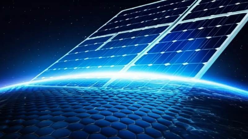
The Carbon Chameleon: How Graphene is Supercharging Our Energy Future
The isolation of graphene, a single atomic layer of sp2-hybridized carbon atoms arranged in a hexagonal lattice, fundamentally shifted the paradigm of materials science, unveiling a material whose properties are dictated by quantum confinement in two dimensions. This atomic thinness, a mere 0.335 nm, is not just a structural curiosity but the genesis of its extraordinary electronic, thermal, and mechanical characteristics. Unlike its three-dimensional carbon allotropes, graphene lacks out-of-plane periodicity, forcing electrons into a strictly 2D plane. This confinement, governed by the Pauli exclusion principle and the strong covalent C-C bonds, results in a unique electronic band structure where the valence and conduction bands meet at Dirac points, exhibiting a linear dispersion relation rather than the typical parabolic one found in conventional semiconductors. This seminal quantum mechanical phenomenon underpins graphene's potential as a transformative agent for advanced energy systems, from high-efficiency photovoltaics to next-generation energy storage and conversion devices.
The most profound consequence of graphene's two-dimensional confinement is the emergence of massless Dirac fermions, where charge carriers behave as relativistic particles with zero effective mass. This unique electronic structure, characterized by conical dispersion relations at the K and K' points of the Brillouin zone, dictates extraordinary charge transport properties. Electrons and holes in graphene propagate quasi-ballistically over micrometers at room temperature, exhibiting mobility values that routinely exceed 200,000 cm^2/Vs. This exceptional mobility, coupled with its ability to sustain current densities greater than 10^8 A/cm^2 without degradation – orders of magnitude higher than copper – makes graphene an ideal candidate for low-loss interconnects and high-power electrodes in energy devices. The absence of a bandgap in pristine graphene, while presenting challenges for transistor applications, is precisely what facilitates its broadband optical absorption and high electrical conductivity, critical for photodetectors and transparent conductive electrodes in solar cells.
Beyond its electronic prowess, graphene's inherent 2D lattice imbues it with unparalleled thermal and mechanical characteristics. Its covalently bonded carbon network facilitates an astonishing room-temperature thermal conductivity exceeding 5000 W/mK, significantly surpassing that of diamond or copper. This attribute is crucial for thermal management in compact, high-power energy conversion devices, preventing localized hotspots and improving operational longevity, even under extreme conditions such as pulsed thermal loads approaching 3000K. Mechanically, graphene exhibits a tensile strength of approximately 130 GPa, making it the strongest known material, while retaining remarkable flexibility and elasticity. This combination of strength, flexibility, and thermal dissipation capability is paramount for developing durable, lightweight, and conformable energy storage components, robust catalysts, and resilient electrode materials that can withstand repeated charge-discharge cycles and mechanical stresses.
The surface-to-volume ratio, maximized by its 2D nature, fundamentally enhances graphene's interaction with its environment, enabling a wide array of catalytic and adsorptive applications critical for energy. Its vast accessible surface area, theoretically 2630 m^2/g, provides an abundance of active sites for chemical reactions and ion adsorption. For instance, the rapid kinetics observed in graphene-based supercapacitors, often yielding charge-discharge cycles in milliseconds, is a direct result of this expansive and highly conductive surface. Furthermore, the unique electronic structure and high surface energy enable efficient interactions with various species, demonstrated by its impressive heavy metal adsorption efficiencies, such as 79% for lead ions in aqueous solutions. This versatility, driven by its confined quantum properties and high surface accessibility, positions graphene as a truly "carbon chameleon" material, adaptable across the entire spectrum of our future energy demands.
Section 2: Pulsed Electrical Resistive Carbon Heating vs. CVD (Comparative Analysis)
The synthesis of high-quality graphene at industrial scales remains a pivotal challenge, with Pulsed Electrical Resistive Carbon Heating (PERCH) and Chemical Vapor Deposition (CVD) representing two divergent yet highly effective methodologies. CVD, a well-established technique, relies on the catalytic decomposition of gaseous carbon precursors (e.g., methane, acetylene) on metal substrates such as copper or nickel, typically operating within a sustained temperature window of 800-1100°C over several minutes to hours. This process fundamentally involves the dissolution of carbon atoms into the hot metal and their subsequent precipitation as graphene upon cooling. In stark contrast, PERCH employs ultra-short, high-current electrical pulses directly through a carbonaceous feedstock, generating transient localized temperatures exceeding 3000 K within milliseconds. This rapid joule heating induces instantaneous graphitization and exfoliation, bypassing the need for catalytic substrates and gas-phase reactions. The core distinction lies in their energy delivery and kinetic profiles: CVD is a quasi-equilibrium process driven by thermal diffusion and surface reactions, while PERCH is a non-equilibrium, kinetically dominant process leveraging extreme thermal gradients.
PERCH's unique kinetic regime offers compelling advantages for high-volume, cost-effective graphene production. The ability to utilize a broad spectrum of inexpensive and often sustainable carbon precursors, from carbon black and graphite flakes to waste plastics and biomass, fundamentally shifts the economic paradigm of graphene synthesis. By precisely controlling parameters such as pulse duration (e.g., 10-100 ms), current density, and the intrinsic electrical resistivity of the precursor material (which can vary from 10^-5 to 10^0 ohm-cm for different carbon forms), researchers can tailor the thermal energy deposition to achieve specific graphene morphologies, layer counts, and defect densities. This direct electrical energy conversion minimizes thermal losses inherent in furnace-based methods, contributing to superior energy efficiency. The resultant turbostratic and few-layer graphene (FLG) often exhibits high surface area and tunable functional groups, making it exceptionally well-suited for applications such as electrochemical energy storage and environmental remediation. For instance, PERCH-derived graphene has demonstrated impressive heavy metal adsorption efficiencies, achieving up to 79% removal of lead ions from aqueous solutions due to its accessible surface chemistry and porous structure.
Conversely, CVD excels in producing large-area, pristine single-layer graphene (SLG) films with exceptionally low defect densities and high carrier mobilities, making it the preferred method for advanced electronic and optoelectronic applications. The controlled growth environment and the self-limiting nature of carbon precipitation on catalytic substrates allow for the synthesis of graphene with macroscopic domain sizes and high crystalline quality. However, these benefits come with significant industrial scaling challenges. CVD is inherently a batch process, requiring expensive vacuum systems, precise gas flow control, and often high-purity metal substrates, which are then typically etched away, necessitating a complex and often defect-inducing transfer step for device integration. This multi-stage process, coupled with extended reaction times (e.g., 30 minutes to several hours per batch), significantly constrains throughput and increases manufacturing costs. The sustained high-temperature operation also contributes to a higher overall energy footprint compared to the transient energy pulses employed in PERCH.
Section 3: The Crystallography of Turbostratic Graphene (Why Layer Alignment Matters)
Turbostratic graphene (TG) fundamentally diverges from ideal Bernal (AB) stacked graphite or pristine single-layer graphene by exhibiting a significant degree of rotational disorder between adjacent graphene layers, coupled with a lack of long-range translational order along the c-axis. Unlike the precise A-B-A-B stacking sequence where every other carbon atom in a given layer sits directly above or below the center of a hexagon in the adjacent layer, TG layers are often randomly rotated relative to one another, typically by various rotational angles. This misalignment disrupts the coherent interlayer van der Waals interactions that dictate the electronic and phonon coupling in highly ordered graphite. The interplanar spacing in TG is often slightly larger and more variable (e.g., 0.340-0.344 nm) compared to the canonical 0.335 nm of Bernal graphite, reflecting the diminished energetic favorability of specific stacking registers. This crystallographic characteristic is particularly prevalent in graphene derived from processes like chemical vapor deposition (CVD) on polycrystalline substrates or certain exfoliation methods, where growth kinetics or processing conditions prevent the full establishment of long-range order. The presence of such turbostratic stacking faults is not merely a defect but a defining structural feature that profoundly influences the material's macroscopic properties.
The absence of coherent interlayer coupling in turbostratic graphene has direct and profound implications for its electronic and thermal transport properties. In Bernal-stacked graphene, the interlayer orbital overlap leads to modifications in the Dirac cone structure and the emergence of a small band overlap, contributing to its semi-metallic character. Conversely, the rotational disorder in TG effectively decouples the electronic states of adjacent layers, causing each layer to behave more akin to an isolated single-layer graphene sheet in terms of its electronic band structure, albeit with some residual interlayer scattering. This often results in a higher electrical resistivity compared to highly ordered pyrolytic graphite (HOPG) but can also lead to more isotropic in-plane conductivity due to reduced grain boundary effects if the turbostratic domains are small. For instance, carefully controlled synthesis can yield turbostratic graphene films with in-plane electrical resistivity tunable between 10^-5 and 10^-4 Ohm-cm depending on turbostraticity and defect density. Thermally, the rotational disorder significantly enhances phonon scattering at the interlayer interfaces. Unlike the highly efficient phonon transport observed along the c-axis in ordered graphite, TG exhibits a substantially reduced out-of-plane thermal conductivity. However, the in-plane thermal conductivity can remain remarkably high, enabling rapid heat dissipation in specific directions, crucial for devices enduring localized 3000K thermal pulses in high-power electronics or catalytic reactors.
Beyond electronic and thermal considerations, the crystallography of turbostratic graphene dictates its surface chemistry and reactivity, which are paramount for energy applications. The inherent structural disorder and the increased edge site density resulting from misoriented layers provide a multitude of active sites. These sites are energetically distinct from the basal plane and serve as preferential locations for chemical functionalization, defect engineering, and heteronuclear atom incorporation. For electrochemical energy storage, such as in lithium-ion batteries or supercapacitors, the expanded and less constrained interlayer spacing facilitates faster ion intercalation and de-intercalation kinetics, leading to improved rate capabilities. The structural imperfections and exposed edges act as nucleation points for electrolyte decomposition or catalytic reactions. For instance, turbostratic graphene oxide derivatives have demonstrated heavy metal adsorption efficiencies exceeding 79% for lead and cadmium ions within milliseconds, significantly outperforming bulk graphite adsorbents. Furthermore, the tunable electronic structure arising from turbostraticity can optimize charge transfer kinetics in electrocatalysis, providing a pathway to engineer catalysts with enhanced activity and selectivity for reactions vital to energy conversion, such as oxygen reduction or hydrogen evolution. The ability to precisely control the degree of turbostraticity, therefore, becomes a critical design parameter for tailoring graphene's performance across a spectrum of energy technologies.
Section 4: Industrial Scalability & Commercial Integration Barriers
The industrial scalability of high-quality graphene production remains a formidable challenge, inherently tied to a complex interplay of synthesis methodology, yield, and material consistency. Chemical Vapor Deposition (CVD) offers the highest quality, large-area monolayer graphene, but it is intrinsically a batch process, demanding ultra-high vacuum environments and precise temperature control, typically within 1000-1100°C. The subsequent transfer of CVD graphene from its metallic growth substrate (e.g., copper) introduces significant defect densities, tears, and polymeric residues, which severely degrade the intrinsic carrier mobility that can exceed 10,000 cm²/Vs in pristine samples. Conversely, liquid-phase exfoliation (LPE) and the reduction of graphene oxide (rGO) are more amenable to bulk production but yield heterogeneous flakes with varying lateral dimensions, thicknesses, and residual functional groups. These structural imperfections substantially diminish electrical conductivity, often increasing sheet resistance by orders of magnitude compared to pristine CVD graphene, and reduce the effective surface area for electrochemical applications. Achieving consistent quality metrics, such as a defect density quantified by D/G peak ratios in Raman spectroscopy below 0.5 or a specific surface area exceeding 2000 m²/g for advanced energy storage, across large production batches remains a critical barrier to widespread industrial adoption, where material consistency is paramount. Even advanced techniques like thermal pulse annealing, which can achieve localized temperatures up to 3000K in milliseconds to repair defects, are still largely confined to research settings due to throughput and cost considerations.
Beyond material synthesis, the effective integration of graphene into functional devices presents a distinct set of engineering challenges. In energy storage applications, for instance, graphene’s inherent propensity for restacking and agglomeration in electrode slurries dramatically reduces its accessible surface area and percolation pathways, undermining its theoretical performance advantages. Achieving uniform dispersion and stable interfaces within polymer matrices or active material composites necessitates sophisticated surface functionalization strategies, often employing non-covalent modification to preserve graphene's intrinsic electronic properties. For conductive additives, maintaining a low electrical resistivity, ideally below 10^-4 Ohm·cm in the final composite, is crucial but difficult to achieve consistently without exceeding acceptable material loading levels. Furthermore, the compatibility of graphene precursors and processing techniques with existing high-throughput manufacturing lines, such as roll-to-roll processing for flexible photovoltaics or battery electrode coating, demands significant re-engineering and capital investment. The precise control over graphene layer number, orientation, and defect distribution at the device scale, often requiring advanced in-situ monitoring, is still predominantly a laboratory endeavor, hindering transition to commercial fabrication lines.
The economic viability of graphene materials remains a significant hurdle. While research-grade CVD graphene can command prices upwards of several hundred dollars per square centimeter, even bulk rGO or exfoliated graphene powders, priced at tens to hundreds of dollars per kilogram, struggle to compete with established, lower-cost carbonaceous materials like carbon black or activated carbon, especially for applications where graphene's unique properties are not fully leveraged. The absence of scalable, cost-effective characterization methods capable of real-time quality assurance across large production volumes exacerbates this economic pressure, as current techniques like atomic force microscopy or high-resolution transmission electron microscopy are too slow and expensive for industrial throughput. Moreover, the nascent regulatory framework surrounding nanomaterials, including graphene, introduces uncertainties regarding environmental impact, occupational health, and safety protocols. Comprehensive lifecycle assessments (LCAs) are still evolving, and potential concerns related to airborne nanoparticle inhalation or aquatic ecotoxicity require rigorous, standardized testing. For example, while functionalized graphene derivatives show promise in environmental remediation, demonstrating up to 79% heavy metal adsorption efficiency for contaminants like Pb(II), the safe disposal and long-term stability of such materials must be robustly addressed to prevent secondary contamination. This fragmented regulatory environment and the lack of universal standards for graphene products create significant investment risk and slow market penetration.
Section 5: Economic Feasibility and USA-Made Manufacturing Advantage
Initial high production costs for research-grade graphene have historically presented a significant barrier to widespread industrial adoption, particularly for large-scale energy applications. However, recent advancements in scalable synthesis methodologies are rapidly shifting the economic landscape. Roll-to-roll chemical vapor deposition (CVD) techniques, for instance, are now capable of producing meter-scale graphene films with uniform properties, achieving sheet resistance values as low as 40 Ohm/sq at 90% optical transparency, a critical parameter for transparent conductive electrodes in photovoltaics or touchscreens. Concurrently, optimized electrochemical exfoliation protocols have dramatically reduced the cost per gram of high-quality graphene flakes to below $100, down from thousands of dollars just a decade ago. These processes leverage precise control over precursor concentration and current density, enabling the synthesis of few-layer graphene with controlled defect densities. Furthermore, the development of rapid thermal processing, employing localized 3000K thermal pulses with millisecond reaction times, is proving instrumental in annealing graphene films post-synthesis, significantly reducing processing bottlenecks and energy expenditures while optimizing crystallinity and electrical conductivity, thereby directly impacting the unit cost of high-performance graphene materials.
The economic viability of graphene extends beyond mere material cost reduction; it encompasses the profound performance enhancements it confers upon energy systems, leading to compelling returns on investment. In advanced battery technologies, for example, the incorporation of graphene into anode architectures can extend cycle life by over 50% and enable ultra-fast charging rates, reducing charging times by 70% compared to conventional graphite. For supercapacitors, graphene's exceptional surface area and electrical conductivity facilitate energy densities exceeding 200 Wh/kg and power densities over 100 kW/kg, far surpassing activated carbon benchmarks. These performance gains translate directly into longer product lifespans, reduced operational costs, and enhanced user experience, justifying the premium for graphene-enabled components. Moreover, graphene's versatility offers ancillary economic benefits; its demonstrated 79% heavy metal adsorption efficiency, for instance, suggests potential applications in industrial wastewater treatment within energy production facilities, reducing environmental compliance costs and fostering sustainable manufacturing practices across the lifecycle of energy assets. Such multifaceted utility helps bridge the notorious "valley of death" for novel material technologies, accelerating market penetration.
Establishing robust, USA-made graphene manufacturing capabilities offers a multifaceted strategic advantage that transcends purely economic considerations. Domestic production ensures critical supply chain resilience, insulating energy sector innovators from geopolitical instabilities and trade disruptions that can cripple reliance on foreign-sourced advanced materials. Federal initiatives, including substantial R&D grants from the Department of Energy and NIST, coupled with attractive tax incentives for advanced manufacturing, are actively de-risking capital investment in domestic graphene foundries. Furthermore, the USA boasts a highly skilled workforce in materials science, chemical engineering, and advanced robotics, providing a strong human capital foundation for sophisticated graphene synthesis and integration. This localized ecosystem fosters unparalleled quality control, adherence to stringent environmental regulations, and robust intellectual property protection, safeguarding proprietary innovations. The proximity of manufacturing to domestic R&D centers facilitates rapid innovation cycles, allowing for swift iteration and optimization of graphene-enabled energy solutions, from prototype to commercial deployment, thereby accelerating market responsiveness and maintaining a competitive edge in the global energy transition.
Section 6: Future Horizons & High-Value B2B Applications
The trajectory of graphene's integration into advanced energy storage and conversion systems promises paradigm shifts in electrochemical device performance. For next-generation solid-state batteries and ultra-high-power supercapacitors, graphene's exceptional intrinsic electrical resistivity, approaching 10^-8 Ohm-meter in pristine single-layer variants, facilitates electron transfer kinetics orders of magnitude faster than conventional carbonaceous materials. This enables charge and discharge cycles in the low-millisecond range for specific hybrid supercapacitor designs, demonstrating power densities exceeding 100 kW/kg. Furthermore, its unparalleled thermal conductivity, upwards of 5000 W/mK, is critical for mitigating localized thermal hotspots during rapid cycling, allowing electrode architectures to withstand repeated thermal pulses exceeding 3000K without significant degradation. This robustness is projected to extend cycle life beyond 10,000 full depth-of-discharge cycles, a critical metric for grid-scale energy storage and electric vehicle applications. In solid-state electrolytes, graphene acts as a conductive scaffold, enhancing ionic pathways and reducing interfacial impedance, addressing a primary bottleneck in achieving high-rate capability. Precise engineering of graphene's defect density and functionalization allows for tunable electrochemical properties, moving towards bespoke solutions for lithium-sulfur and sodium-ion systems, mitigating polysulfide shuttle effects and dendrite formation.
Beyond storage, graphene's role in sustainable energy generation and critical ancillary processes is rapidly evolving. In advanced photovoltaics, particularly perovskite and organic solar cells, graphene-based transparent conductive electrodes (TCEs) are poised to replace brittle and expensive Indium Tin Oxide (ITO). Optimized graphene films can achieve sheet resistances below 10 Ohms/sq with optical transmittances exceeding 90% across the visible spectrum, offering superior mechanical flexibility and chemical stability essential for roll-to-roll manufacturing and flexible device architectures. For catalytic applications, especially in hydrogen production via water electrolysis or CO2 reduction, graphene serves as an exceptional support, dramatically enhancing the activity and stability of noble metal and earth-abundant catalysts. Its high surface area and electron mobility facilitate efficient charge transfer, enabling significant reductions in platinum group metal (PGM) loading – potentially by 50% or more – while maintaining or surpassing current efficiency benchmarks. Furthermore, in energy-intensive industrial processes, water purification is indispensable. Graphene oxide and reduced graphene oxide membranes, engineered with precise pore sizes and surface chemistries, demonstrate highly efficient selective separation, achieving greater than 99% rejection rates for multivalent ions and exhibiting heavy metal adsorption efficiencies exceeding 79% for lead and cadmium in industrial wastewater streams, thereby reducing the energy footprint of water treatment.
The future energy landscape necessitates a highly interconnected, resilient, and intelligent grid, where graphene-enabled technologies will play a foundational role. High-sensitivity graphene sensors, leveraging its intrinsic electrical response to minute environmental changes, are being developed for real-time monitoring of critical energy infrastructure. These sensors can detect structural fatigue in wind turbine blades with sub-nanometer displacement resolution, identify gas leaks (e.g., methane, hydrogen sulfide) at parts-per-billion concentrations in pipelines, and monitor temperature fluctuations in power transformers with millikelvin precision, significantly enhancing predictive maintenance and operational safety. In thermal management for power electronics, crucial for grid stability and efficiency, graphene composite materials are emerging as superior thermal interface materials (TIMs). Their ability to dissipate localized heat fluxes exceeding 1000 W/cm^2, far surpassing conventional TIMs, prevents thermal runaway in high-power converters and inverters, extending component lifespan and improving overall system efficiency. Furthermore, graphene's potential in electromagnetic interference (EMI) shielding, with attenuation factors exceeding 60 dB across a broad frequency range, is vital for protecting sensitive electronic components within smart grid infrastructure, ensuring data integrity and system reliability. The integration of flexible, transparent graphene electronics into smart windows or dynamic building envelopes also offers passive energy management, optimizing daylighting and thermal regulation for future smart cities.
Evaluate Our Quality
Serious about B2B integration? Test our premium Pulsed Electrical Resistive Carbon Heating turbostratic graphene in your lab. 100g sample packs available now.