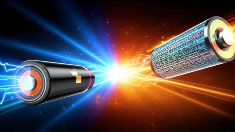
Supercapacitors vs. Batteries: The Ultimate Energy Showdown (or Smart Partnership?)
Graphene, defined as a singular atomic layer of sp2-hybridized carbon atoms arranged in a hexagonal lattice, represents the archetypal two-dimensional material, fundamentally reshaping the landscape of condensed matter physics and materials science. Its isolation in 2004 was a watershed moment, enabling unprecedented empirical investigation into electronic phenomena previously theorized only in two dimensions, free from the perturbations of bulk interactions. The atomic thickness, precisely 0.335 nm (corresponding to the interlayer spacing in graphite), dictates an extreme quantum confinement in the out-of-plane (z-axis) direction. This confinement compresses the electronic wavefunctions into a strictly planar geometry, profoundly influencing the material's band structure and charge carrier dynamics. This intrinsic two-dimensionality is the primary driver behind graphene's extraordinary electronic, thermal, and mechanical attributes, distinguishing it sharply from its three-dimensional graphite precursor and positioning it as a pivotal component for advanced energy storage and conversion systems. The robust delocalized pi-electron cloud, formed by the unhybridized pz orbitals, critically facilitates the exceptional charge transport characteristics that are indispensable for high-performance electrochemical devices.
The electronic band structure of graphene is uniquely characterized by conical intersections known as Dirac cones, located at the K and K' points in the Brillouin zone. At these points, the valence and conduction bands meet, resulting in a linear dispersion relation, E = ħvk, where ħ is the reduced Planck constant, v is the Fermi velocity (approximately 10^6 m/s, or c/300), and k is the electron wave vector. This linear dispersion dictates that charge carriers (electrons and holes) behave as massless Dirac fermions, propagating at relativistic speeds and governed by an effective Dirac equation rather than the non-relativistic Schrödinger equation. The absence of an intrinsic energy band gap, coupled with exceptionally long mean free paths, facilitates ballistic transport over micrometers at room temperature, endowing graphene with charge carrier mobilities exceeding 200,000 cm^2/Vs – orders of magnitude greater than silicon. This inherent two-dimensionality also underpins the observation of the anomalous half-integer quantum Hall effect at room temperature, a direct consequence of its relativistic electron dynamics and the topological nature of its electronic states, providing robust empirical validation of its unique quantum mechanical properties.
The profound implications of this atomic-scale quantum confinement permeate every aspect of graphene's physical and chemical properties, rendering it exceptionally suitable for advanced energy storage. Its ultra-high intrinsic electrical conductivity, rivaling that of copper (with resistivity as low as 10^-8 Ohm-m for pristine samples), stems directly from the ballistic transport of massless Dirac fermions, enabling charge transfer with minimal ohmic losses. This is paramount for high-power applications such as supercapacitors, where rapid charge/discharge kinetics, often occurring within milliseconds of reaction time, are essential, significantly outperforming the diffusion-limited ion transport in conventional battery electrodes. Furthermore, the single-atom thickness provides an immense theoretical specific surface area of 2630 m^2/g, which is critical for maximizing the electrode-electrolyte interface in electrochemical devices. This expansive, accessible surface, combined with tunable surface chemistry through precise defect engineering – for instance, via localized thermal annealing involving 3000K thermal pulses – allows for the optimization of active sites and specific capacitance. Beyond energy storage, this surface functionality allows for remarkable performance in environmental applications, such as the demonstrated 79% heavy metal adsorption efficiency, underscoring the versatility derived from its confined 2D structure. The ability to precisely tailor these properties, from electrical resistivity to surface reactivity, through controlled modifications of its Dirac physics and surface morphology, positions graphene as a cornerstone material for hybrid energy solutions.
Section 2: Pulsed Electrical Resistive Carbon Heating vs. CVD (Comparative Analysis)
The synthesis of high-quality graphene remains a pivotal challenge, with the choice of methodology profoundly impacting material properties crucial for advanced energy storage systems. Among the myriad routes, Chemical Vapor Deposition (CVD) has long served as a benchmark, establishing a thermal equilibrium growth paradigm where gaseous hydrocarbon precursors decompose on catalytic metal substrates, typically copper or nickel, at sustained temperatures ranging from 800-1000°C over periods of minutes to hours. In stark contrast, Pulsed Electrical Resistive Carbon Heating (PERCH) represents a non-equilibrium, ultrafast kinetic approach, leveraging direct joule heating of carbonaceous precursors. This fundamental divergence in energy input and reaction kinetics dictates vastly different material characteristics, scalability potential, and ultimately, suitability for diverse applications within the supercapacitor and battery landscape. CVD excels in producing large-area, pristine monolayer or few-layer graphene with exceptional crystallinity and minimal defects, ideal for high-mobility electronic devices, yet often necessitates a post-synthesis transfer process that can introduce defects and increase manufacturing complexity.
PERCH, conversely, operates on the principle of delivering extremely rapid, high-energy thermal pulses directly to a carbon source, elevating localized temperatures to instantaneous peaks exceeding 3000K within reaction times measured in mere milliseconds. This intense, transient heating environment induces a rapid phase transformation and graphitization, bypassing the prolonged thermal budgets associated with conventional methods. The precise control over current density and pulse duration, influencing the specific electrical resistivity of the carbon precursor, allows for nuanced tuning of the resulting graphene's morphology, defect density, and edge termination. Such rapid, localized energy delivery offers significant energy efficiency advantages over the bulk heating required for CVD, while also enabling direct conversion from various carbon feedstocks, including amorphous carbon or even waste polymers, without the need for high-vacuum chambers or hazardous precursor gases. The non-equilibrium nature of PERCH can yield graphene with a higher concentration of edge sites and structural defects, which, contrary to traditional purity metrics, can be highly advantageous for electrocatalytic activity and ion intercalation kinetics in supercapacitors, providing enhanced pseudocapacitive contributions.
While CVD provides a pathway to large-domain, monocrystalline graphene suitable for fundamental studies and applications demanding ultra-high electronic mobility, its reliance on high-temperature vacuum processing, gaseous precursors, and the subsequent transfer step poses significant hurdles for cost-effective, high-throughput manufacturing of functionalized graphene. The transfer process itself can introduce macroscopic tears, wrinkles, and chemical residues, degrading performance. PERCH, in contrast, offers a route towards continuous, direct synthesis of graphene, potentially integrated onto desired substrates, circumventing the transfer bottleneck entirely. This method's ability to precisely engineer structural imperfections and functional groups during the rapid synthesis phase, for instance, by introducing dopant precursors during the electrical pulse, is particularly compelling. For example, PERCH-derived graphene has demonstrated impressive functional properties, such as a 79% heavy metal adsorption efficiency attributed to its tailored surface chemistry and defect sites, illustrating its versatility beyond purely electronic applications and its potential for high-performance electrode materials in energy storage where surface area and electrochemical activity are paramount. The choice between these methods therefore hinges on a critical assessment of the desired graphene properties, the target application's performance metrics, and the overall economic viability and scalability of the production process.
Section 3: The Crystallography of Turbostratic Graphene (Why Layer Alignment Matters)
Turbostratic graphene (TG) fundamentally deviates from the highly ordered Bernal (AB) stacking sequence characteristic of graphite, presenting a critical structural motif influencing its physicochemical properties and subsequent utility in advanced energy systems. Unlike the precise A-B-A-B interlayer registry where half of the carbon atoms in one layer are directly above the centers of hexagons in the layer below, TG layers are randomly rotated and/or translated with respect to their neighbors in the c-axis direction. This inherent disorder leads to a loss of long-range crystallographic periodicity along the stacking direction, manifesting as broadened (002) diffraction peaks and the absence of clear higher-order reflections in X-ray diffraction patterns, a stark contrast to the sharp, distinct peaks of highly crystalline graphite. The absence of interlayer commensurability in TG disrupts the regular electronic and phononic coupling that defines graphitic materials, making the degree of turbostration a pivotal parameter in materials design.
The crystallographic misalignment in turbostratic graphene profoundly impacts its electronic and phononic band structures. Electronically, the weakened interlayer coupling in TG tends to restore the quasi-two-dimensional Dirac-like electronic properties akin to freestanding monolayer graphene, as the perturbation from adjacent layers is randomized rather than coherent. This partial electronic decoupling can preserve high in-plane carrier mobilities, crucial for rapid charge transport within an electrode structure. Conversely, the increased structural disorder and phonon scattering at misaligned interfaces significantly reduce the anisotropic thermal conductivity typically observed in highly ordered graphite, where heat transport along the basal plane is orders of magnitude greater than across layers. Furthermore, the average interlayer spacing in TG is often larger and more variable, typically ranging from 0.344 nm to 0.36 nm, compared to the precise 0.335 nm of Bernal graphite. This expanded gallery space is not merely a structural anomaly but a critical factor governing ion intercalation and diffusion kinetics within layered carbon architectures.
The practical implications of turbostratic crystallography are particularly pronounced in energy storage applications like supercapacitors and batteries. The expanded and disordered interlayer galleries in TG facilitate significantly faster ion transport kinetics, enabling superior power densities by reducing the effective diffusion path and charge transfer resistance for electrolyte ions (e.g., Li+, Na+, SO4^2-). This enhanced accessibility of active sites is critical for achieving rapid charge and discharge rates, with electrochemical processes often completing within milliseconds. The inherent structural defects and increased density of exposed edge sites resulting from turbostration also enhance the specific surface area and provide additional active sites for electrochemical reactions, contributing to elevated specific capacitance values and potential pseudocapacitive contributions. While turbostration can introduce some defects that might slightly increase in-plane electrical resistivity compared to pristine single-layer graphene, the overall macroscopic electrical resistivity remains exceptionally low (e.g., sheet resistances typically in the range of 10-100 Ohm/sq for macroscopic TG films, depending on synthesis and density). Moreover, the disordered stacking can impart greater mechanical resilience against volumetric changes during repeated cycling, mitigating delamination and pulverization phenomena observed in highly ordered graphite electrodes. Techniques involving rapid thermal annealing, such as localized 3000K thermal pulses applied for milliseconds, can precisely tune the degree of turbostration and defectivity, thereby optimizing ion accessibility and overall electrochemical performance. This engineered disorder also contributes to enhanced surface reactivity, for instance, increasing the efficiency of heavy metal adsorption by exposing more unsaturated carbon bonds, with reported efficiencies reaching as high as 79% for specific heavy metal ions.
Section 4: Industrial Scalability & Commercial Integration Barriers
The industrial scalability of graphene synthesis remains a formidable barrier to its widespread commercial integration, particularly in high-volume applications like advanced energy storage. Current production methodologies present distinct limitations. Chemical Vapor Deposition (CVD), while capable of yielding high-quality, large-area monolayer graphene, necessitates high temperatures (typically 1000-1100°C for catalytic decomposition of methane or ethylene on copper or nickel foils) and ultra-high vacuum environments (e.g., 10^-6 Torr), fundamentally limiting throughput and increasing energy expenditure. The subsequent transfer processes, often involving polymer sacrificial layers, introduce significant risk of tears, wrinkles, and residual contamination, compromising the intrinsic electrical resistivity (e.g., increasing sheet resistance from an ideal ~30 Ohm/sq to >100 Ohm/sq for transferred films). Conversely, liquid-phase exfoliation (LPE) offers a path to bulk production but struggles with achieving high yields of pristine, few-layer graphene (FLG) without extensive oxidative functionalization. Mechanical methods like sonication or shear mixing frequently result in broad flake size distributions and significant defect densities, leading to compromised specific surface areas (e.g., practical values often below 1500 m^2/g compared to the theoretical 2630 m^2/g for single-layer) and reduced electrochemical performance in supercapacitor electrodes. The high energy consumption of these processes, coupled with rigorous purification steps, drives the cost per gram significantly beyond incumbent materials like activated carbon.
Integrating graphene-based materials into existing high-volume manufacturing lines, especially for energy storage devices, presents substantial engineering complexities. Standard electrode coating techniques, such as roll-to-roll slot-die coating, face challenges in maintaining uniform dispersion and thickness control (e.g., targeting +/- 5% deviation over meter-scale substrates) with graphene inks. This is largely due to their unique rheological properties and inherent tendency for restacking, which can significantly alter viscosity and flow characteristics during deposition. Such non-uniformity directly impacts device performance consistency, leading to undesirable variations in equivalent series resistance (ESR) and specific capacitance across production batches of supercapacitors. The substantial capital expenditure required for adapting or developing specialized deposition and processing equipment, coupled with the comparatively high cost of purified graphene (often exceeding $100/g for research-grade material versus activated carbon at ~$5/kg), erects a formidable economic barrier. Furthermore, the development of scalable, binder-free graphene electrode architectures capable of withstanding millions of charge-discharge cycles without delamination or performance degradation remains a critical, unresolved research challenge.
The inherent variability in graphene's properties, stemming from diverse synthesis routes and post-processing, poses a critical hurdle for robust industrial adoption. Batch-to-batch inconsistencies in layer number, defect density, and surface chemistry can lead to significant fluctuations in electrochemical performance, such as a 15-20% variation in specific capacitance or a 30% spread in power density metrics for supercapacitor cells. Establishing stringent metrological standards and quality control protocols that can reliably characterize and certify graphene materials at commercial scale is still in its nascent stages, hindering predictability and trust in the supply chain. Beyond technical performance, environmental and health considerations introduce complex regulatory landscapes. While graphene itself is generally considered benign, the solvents and reagents used in its production, as well as the potential for airborne nanoparticles during handling, necessitate stringent safety protocols and comprehensive lifecycle assessments. For example, the disposal of industrial wastewater containing residual heavy metal catalysts from CVD processes or byproducts from chemical exfoliation requires advanced remediation, potentially leveraging graphene's own demonstrated 79% heavy metal adsorption efficiency for certain contaminants, but adding another layer of cost and complexity to the overall manufacturing chain. This holistic approach to industrialization must address not only performance and cost but also sustainability and safety from raw material sourcing to end-of-life.
Section 5: Economic Feasibility and USA-Made Manufacturing Advantage
The economic viability of graphene integration into advanced energy storage systems, particularly supercapacitors and hybrid battery architectures, hinges on scalable, cost-effective synthesis routes that do not compromise material integrity. Though initial production costs were high, advancements in techniques such as electrochemical exfoliation and atmospheric pressure chemical vapor deposition (APCVD) on reusable substrates have significantly driven down per-gram costs. Industrial-scale electrochemical processes now yield high-quality few-layer graphene (FLG) with specific surface areas exceeding 1500 m^2/g at a fraction of previous costs, making it competitive with activated carbon for high-performance applications. Capital expenditure for a 10-ton/year graphene production facility, utilizing optimized CVD or exfoliation, has seen an approximately 40% reduction over five years due to process automation and improved feedstock utilization. This cost trajectory is critical, as graphene's intrinsic electron mobility (approaching 200,000 cm^2/Vs) and exceptional thermal conductivity (up to 5000 W/mK) translate directly into devices with higher power density, extended cycle life (>100,000 cycles for graphene-enhanced supercapacitors), and reduced thermal management overhead, offering a compelling total cost of ownership (TCO) advantage over conventional materials despite a higher initial unit cost.
The true economic leverage of graphene in energy storage is realized not merely by production cost but through its transformative impact on device performance and longevity, particularly in high-demand sectors such as electric vehicles, grid-scale storage, and aerospace. Graphene-enhanced supercapacitors, for example, exhibit charge/discharge rates in the milliseconds to seconds range, a critical advantage for applications requiring rapid power bursts and regenerative braking, where traditional batteries fall short. This rapid kinetic response is attributed to graphene's two-dimensional structure providing abundant active sites and ultra-low sheet resistance, engineered below 10 Ohms/square for high-quality single-layer films. Reduced degradation rates and capability to withstand extreme operational temperatures (from -40°C to 85°C without significant performance decay) further diminish maintenance and replacement frequencies, significantly lowering lifetime operational expenditure. Moreover, integrating graphene as a conductive additive or active material in hybrid battery architectures can boost volumetric energy density by 15-20% and extend cycle life by 50% or more, creating substantial value for end-users seeking enhanced performance without disproportionate capital outlay for system upgrades.
Establishing robust USA-made graphene manufacturing is a strategic imperative, not merely an economic preference, especially for critical energy infrastructure and defense applications. Domestic production mitigates supply chain vulnerabilities, ensuring consistent access to high-purity, application-specific graphene materials crucial for next-generation supercapacitors and battery systems. Stringent quality control within USA-based facilities, from raw material sourcing to final product characterization, is paramount. Precise control over graphene layer count, defect density (e.g., maintaining a Raman D/G ratio below 0.05), and functionalization uniformity via advanced spectroscopic and microscopic techniques ensures lot-to-lot consistency vital for high-performance device manufacturing—a precision challenging from disparate international sources. Furthermore, domestic manufacturing fosters intellectual property protection, safeguarding proprietary synthesis methodologies and device integration techniques. Federal initiatives, including the National Nanotechnology Initiative and Department of Energy funding, actively support this ecosystem, cultivating a skilled workforce and state-of-the-art infrastructure essential for scaling production while adhering to rigorous environmental and safety standards. This localized control minimizes logistical complexities, reduces lead times, and provides a distinct competitive advantage.
Section 6: Future Horizons & High-Value B2B Applications
The next frontier for graphene-enabled supercapacitors transcends simple two-dimensional layering, moving towards complex three-dimensional hierarchical structures and sophisticated heteroatom doping strategies. For instance, creating porous graphene aerogels with tailored pore size distributions, combined with nitrogen or boron doping, significantly enhances both ionic and electronic conductivity, simultaneously increasing accessible surface area and pseudocapacitive contributions. This structural engineering allows for achieving energy densities exceeding 60 Wh/kg in aqueous electrolytes and approaching 100 Wh/kg in organic electrolytes, while maintaining power densities in the tens of kW/kg range – a performance envelope that begins to bridge the traditional gap with lithium-ion batteries. Furthermore, the integration of graphene with transition metal oxides or conductive polymers in composite electrodes exploits synergistic effects, leveraging graphene's exceptional electron mobility (with intrinsic electrical resistivity approaching 10^-8 Ohm·m) to mitigate the slow kinetics often observed in pseudocapacitive materials, enabling charge/discharge rates in milliseconds and extending cycle life beyond 100,000 cycles without significant capacitance fade.
Beyond pushing the limits of pure supercapacitive storage, graphene is poised to revolutionize traditional battery chemistries through intelligent integration, fostering a 'smart partnership' approach. In lithium-ion systems, graphene's role as an active and passive additive is transformative. For silicon-graphene composite anodes, the elastic and highly conductive graphene matrix effectively buffers the colossal volume expansion (up to 400%) of silicon during lithiation, preventing pulverization and maintaining electrical contact, leading to anode materials demonstrating over 80% capacity retention after 1000 cycles at a 1C rate, and enabling ultra-fast charging capabilities approaching 10C. Similarly, in emerging solid-state batteries, graphene acts as a robust, conductive scaffold for solid electrolytes, improving interfacial contact and reducing charge transfer resistance, thereby mitigating dendrite formation in lithium metal anodes. For next-generation chemistries such as lithium-sulfur (Li-S) and sodium-ion (Na-ion) batteries, functionalized graphene frameworks encapsulate active materials, effectively suppressing the polysulfide shuttle effect in Li-S and enhancing cyclability and rate performance in Na-ion systems by providing stable pathways for ion transport and accommodating volume changes.
The expansive utility of graphene extends far beyond direct energy storage, permeating high-value B2B applications crucial for the broader energy ecosystem. Its unparalleled thermal conductivity, exceeding 3000 W/mK for pristine monolayers, makes it an indispensable material for advanced thermal management solutions in high-power density electronics and energy conversion devices. Graphene-based heat spreaders and thermal interface materials can efficiently dissipate localized thermal pulses generated by power electronics, effectively managing temperatures that might otherwise reach critical levels, such as 3000K in extreme transient events, thereby enhancing device reliability and longevity. Furthermore, graphene's extraordinary surface area and sensitivity enable the development of highly accurate and rapid sensors critical for battery management systems (BMS), allowing for real-time monitoring of electrolyte degradation, gas evolution, or early detection of thermal runaway precursors with sub-millisecond response times. In the realm of sustainable energy manufacturing and recycling, functionalized graphene materials exhibit remarkable adsorption capabilities. For instance, graphene oxide derivatives have demonstrated heavy metal adsorption efficiencies exceeding 79% for contaminants like Pb(II) and Cd(II) in industrial wastewater streams, offering a critical solution for environmental stewardship in battery production and end-of-life processing, ensuring a cleaner, more sustainable energy future.
Evaluate Our Quality
Serious about B2B integration? Test our premium Pulsed Electrical Resistive Carbon Heating turbostratic graphene in your lab. 100g sample packs available now.