SiC Sublimation Graphene: High-Quality Production for Electronics
Graphene, a single layer of hexagonally ordered carbon atoms, has revolutionized the materials science landscape with its extraordinary electronic, mechanical, and thermal properties. Its potential applications span from ultra-fast transistors and transparent electrodes to advanced sensors and energy storage devices. However, realizing this potential hinges critically on the ability to produce high-quality, large-area graphene uniformly and reproducibly.
While various methods exist for graphene production, each comes with its own set of advantages and limitations. For the burgeoning fields of microelectronics and nanoelectronics, where precision and scalability are paramount, the demand for exceptionally consistent material is non-negotiable. This necessitates advanced synthesis techniques that can deliver on these stringent requirements.
Among the most promising approaches is the high-temperature sublimation of silicon carbide (SiC) in vacuum, a sophisticated epitaxial method that stands out for its capacity to yield high-quality graphene films with easily controllable thickness and remarkable reproducibility across entire wafer surfaces. This process is not merely an academic curiosity but a cornerstone technology driving the development of next-generation electronic devices, offering a pathway to integrate graphene seamlessly into existing semiconductor infrastructures.
Graphene Production Unveiled: A Comparative Look at Synthesis Methods
The journey to harness graphene's unique properties begins with its effective production, a challenge that has spurred innovation across several distinct methodologies. Broadly, these can be categorized into three main groups: mechanical, chemical, and epitaxial methods. Each approach offers a unique balance of cost, quality, and scalability, dictating its suitability for different applications and research objectives.
Mechanical methods, epitomized by the Scotch tape technique, involve the physical exfoliation of graphene from pyrolytic graphite crystals. These methods are celebrated for their simplicity and low cost, capable of producing relatively large-area samples, often up to 100 µm. However, their primary drawbacks—nonuniform thickness and the notoriously difficult transfer procedure onto various substrates—significantly hinder their widespread industrial adoption, particularly for precision electronic components.
Chemical methods, such as chemical vapor deposition (CVD) and reduction of graphene oxide, represent another significant group. These techniques are often distinguished by their high yield of material and potential for scalability. Yet, they frequently struggle with producing samples of sufficiently large dimensions or maintaining the pristine structural integrity required for high-performance electronics. The presence of defects or residual contaminants can critically impair graphene's intrinsic properties, limiting its utility in sensitive applications.
In contrast, epitaxial methods, including the thermal dissociation of silicon carbide wafers, offer a compelling alternative. This group is uniquely positioned to address the limitations of mechanical and chemical approaches by providing films with easily controllable thickness and exceptional reproducibility of parameters across the entire wafer surface. For the rigorous demands of microelectronic and nanoelectronic device development, the precision and consistency offered by SiC sublimation graphene are not just advantageous, but often indispensable, making it a focal point for advanced materials research and industrial implementation.
The Epitaxial Edge: Why SiC Sublimation is Key for Advanced Electronics
The pursuit of high-performance electronic devices necessitates materials with impeccable structural integrity and precise control over their fundamental properties. This is where epitaxial methods, particularly the high-temperature sublimation of silicon carbide, demonstrate their profound advantage. Unlike other graphene synthesis techniques, SiC sublimation offers a pathway to intrinsic material quality directly compatible with semiconductor manufacturing processes, making it a preferred choice for cutting-edge applications.
One of the paramount benefits of this method is its ability to produce graphene films with easily controllable thickness. This precision is crucial for designing and fabricating devices where the number of graphene layers directly influences electronic behavior, such as in field-effect transistors or quantum computing components. Engineers can tailor the growth parameters to reliably achieve single-layer, bilayer, or few-layer graphene, ensuring the desired electrical characteristics for specific device architectures. This level of control is rarely matched by other large-scale production techniques.
Furthermore, the silicon carbide thermal dissociation process ensures high reproducibility of parameters across the entire surface of the wafer. This uniformity is a cornerstone for industrial scalability and the mass production of reliable electronic components. For manufacturers producing thousands or millions of chips, consistent material properties from one wafer to the next, and even within different regions of a single wafer, are absolutely essential. The inherent nature of epitaxial growth on a crystalline substrate provides this critical consistency, minimizing variations that could lead to device failure or performance degradation.
Consequently, it is this group of methods, with SiC sublimation graphene at its forefront, that garners the most interest for the development of technologies in microelectronic and nanoelectronic devices. The ability to grow high-quality graphene directly on a semiconductor substrate, often leveraging existing SiC wafer technology, streamlines integration and reduces fabrication complexities. This strategic advantage positions SiC sublimation as a cornerstone technology for unlocking the full potential of graphene in future generations of high-performance electronics.
Deconstructing Silicon Carbide Thermal Dissociation: The Sublimation Mechanism
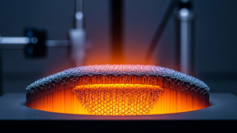
At the heart of SiC sublimation graphene formation lies the intricate process of silicon carbide thermal dissociation in a vacuum. This method harnesses the differential evaporation rates of silicon and carbon atoms from the SiC crystal lattice at elevated temperatures, leaving behind a carbon-rich surface that reorganizes into graphene. Understanding the precise chemical and physical phenomena occurring during this sublimation is crucial for controlling the quality and characteristics of the resulting graphene layers.
Research conducted using mass spectroscopy has definitively shown that during the sublimation of silicon carbide, the primary evaporated components are SiC, Si, Si2C, and SiC2. This complex mixture of vapor species dictates the kinetics of the surface transformation. A comprehensive thermodynamic analysis of this sublimation process and the calculation of vapor composition were pioneered by research led by Yu. M. Tairov at St. Petersburg Electrotechnical University (LETI). This foundational work was instrumental in developing the technology for SiC ingot production via physical vapor deposition (PVD), a process now globally adopted by major manufacturers.
It is important to note that the conditions of sublimation are critical. If the external pressure exceeds the saturation pressure of silicon vapor, all components involved in the dissociation reaction of SiC tend to remain in the condensed phase. However, in a vacuum, or under controlled low-pressure inert atmospheres, the silicon preferentially evaporates. A critical thermodynamic threshold for the complete decomposition of silicon carbide is established at temperatures greater than 3150 K. At these extreme temperatures, the Gibbs free energy change (ΔG₀) becomes negative, indicating that the reaction SiC(sol) ⇔ Si(liq) + C(sol) proceeds spontaneously, leading to the complete breakdown of the SiC solid phase into liquid silicon and solid carbon.
Below this limiting temperature, specifically within the broad range of 1500–3100 K, the process of dissociative evaporation of silicon carbide can be represented by a set of simultaneous reactions. These reactions, each with its own equilibrium constant (Kᵢ) and partial pressure (Pᵢ) of the components, govern the exact composition of the vapor phase and the rate at which carbon accumulates on the surface. Understanding these equilibrium dynamics is essential for precise control over the graphene growth environment and the resulting film properties.
The Chemistry of Graphene Formation: Vapor Dynamics and Residual Carbon Layer
The formation of a graphene layer on a silicon carbide substrate through thermal dissociation is a sophisticated chemical process governed by a delicate balance of vapor dynamics and surface kinetics. Within the critical temperature range of 1500–3100 K, a series of distinct dissociative evaporation reactions occur, each contributing to the evolving composition of the vapor phase and the accumulation of carbon on the SiC surface. These reactions dictate the rate at which silicon atoms depart, leaving behind a carbon-rich residue that eventually reconfigures into graphene.
Key reactions describing this process include: SiC(sol) ⇔ Si(gas) + C(sol), 2SiC(sol) ⇔ Si2C(gas) + C(sol), 2SiC(sol) ⇔ SiC2(gas) + Si(liq,gas), and SiC(sol) ⇔ SiC(gas). The equilibrium constants (Kᵢ) for these reactions are derived from the isotherms of chemical reactions based on the change in Gibbs free energy (ΔG₀ = -RT ln Kᵢ). By analyzing the partial pressures of Si, Si2C, SiC2, and SiC in closed systems, scientists can precisely assess the specific features of the sublimation process across the entire temperature spectrum, both in vacuum and in neutral media like argon.
In the temperature range up to approximately 2546 K, the partial pressure of free Si in the vapor phase significantly exceeds that of SiC molecules. During this phase, the partial pressure of atomic Si is predominantly determined by the reaction SiC(sol) ⇔ Si(gas) + C(sol), although the formation of Si from 2SiC(sol) ⇔ SiC2(gas) + Si(liq,gas) also occurs simultaneously, albeit to a lesser extent. Crucially, in this lower temperature regime, the pressure of Si vapors remains below saturation pressure, implying that the dissociation and vapor composition formation primarily occur in the vapor phase rather than through condensation. This dynamic ensures a continuous removal of silicon, facilitating carbon accumulation.
As temperatures rise above 2546 K, the reaction 2SiC(sol) ⇔ Si2C(gas) + C(sol) effectively terminates, as its corresponding change in isobaric potential becomes positive (ΔG₀ > 0). Beyond this point, the partial pressure of silicon in the vapor above the SiC surface is primarily controlled by the reaction 2SiC(sol) ⇔ SiC2(gas) + Si(liq,gas). This shift in dominant reaction pathways profoundly influences the rate and mechanism of carbon deposition. Regardless of the specific temperature regime, the fundamental outcome of these dissociative evaporation processes is the accumulation of free carbon in the condensed phase, which gradually forms a residual carbon layer on the surface of the initial SiC phase. This carbon-rich layer then undergoes self-assembly, driven by the high temperatures, to form the highly ordered hexagonal lattice of SiC sublimation graphene.
Precision and Scalability: Engineering High-Quality Graphene on SiC Wafers
The ability to precisely control the formation of graphene layers on silicon carbide wafers is a cornerstone of its application in advanced electronics. The epitaxial nature of SiC sublimation graphene allows for an unprecedented level of control over film thickness, uniformity, and crystalline quality, directly impacting the performance of integrated devices. This precision is not merely an academic achievement but a practical necessity for the semiconductor industry, where material consistency on a wafer scale is paramount.
The thermal dissociation process is carefully engineered to ensure that silicon atoms preferentially sublimate from the SiC surface in a vacuum, leaving behind an excess of carbon atoms. These residual carbon atoms then reconstruct into the stable hexagonal lattice of graphene. The rate of silicon sublimation, and consequently the rate of graphene formation, can be meticulously controlled by adjusting parameters such as temperature, pressure, and the specific crystallographic face of the SiC wafer. For instance, the epitaxial assembly of graphene on the (0001) face of silicon carbide has been extensively studied, demonstrating how different lattice orientations can influence growth kinetics and graphene quality.
This method’s inherent reproducibility over the entire surface of the wafer is a significant advantage for large-scale production. Unlike techniques that might yield patchy or inconsistent graphene layers, SiC sublimation can produce uniform films across commercially relevant wafer sizes, ensuring that every device fabricated on that wafer benefits from consistent material properties. This consistency is vital for manufacturing reliability and yield, which are critical metrics in the fiercely competitive microelectronics market.
Indeed, the technology derived from understanding SiC sublimation, particularly Physical Vapor Deposition (PVD) for SiC ingot production, is already utilized by major global manufacturers. Large-scale corporations such as CREE and Dow Corning (USA), Philips and Siemens (Europe), and Toyota and Sony (Japan) are prominent producers of commercial single-crystal SiC and SiC-based devices. The existing infrastructure and expertise in SiC wafer technology provide a natural synergy for integrating SiC sublimation graphene into the production of next-generation electronic components, from high-frequency transistors to robust power electronics.
Beyond the Lab: Industrial Impact and Future Horizons of SiC Sublimation Graphene
The transition of SiC sublimation graphene from a laboratory phenomenon to an industrially viable production method underscores its profound impact on the future of electronics. Its unique advantages, particularly in terms of quality, reproducibility, and compatibility with existing semiconductor processes, position it as a critical material for enhancing and enabling a new generation of high-performance devices. The ongoing evolution of this technology continues to push the boundaries of what is possible in microelectronics and nanoelectronics.
The ability to produce high-quality, atomically thin graphene films directly on SiC substrates is a game-changer for device integration. This eliminates the often-problematic transfer steps associated with other graphene synthesis methods, which can introduce defects, contamination, or mechanical damage. Direct growth ensures a cleaner interface and superior electrical contact, leading to more reliable and efficient devices. This inherent advantage is why research into the electronic structure and transport properties of these films, as well as the synthesis and characterization of atomically thin graphite films on SiC substrates, remains a vibrant area of scientific inquiry.
Moreover, the scalability of SiC sublimation to commercial wafer sizes means that the benefits of graphene can be realized in mass-produced components. The investment by major corporations in SiC-based technologies creates a fertile ground for the adoption of SiC-grown graphene. This integration could lead to significant advancements in areas such as high-frequency communication, high-power electronics, and extreme environment sensing, where SiC is already a preferred substrate due to its robust properties.
Looking ahead, research continues to refine the SiC sublimation process, exploring methods for even greater control over graphene layer number, defect density, and interface properties. Promising avenues include direct transformation of amorphous SiC into graphene under low temperature and ambient pressure conditions, further expanding the versatility of SiC as a graphene source. These continuous innovations ensure that SiC sublimation graphene will remain at the forefront of advanced materials science, driving the development of smaller, faster, and more powerful electronic devices that will shape our technological future.
SEO FAQ Section
What is SiC sublimation graphene?
SiC sublimation graphene is a form of graphene produced by heating a silicon carbide (SiC) wafer to high temperatures in a vacuum. During this process, silicon atoms preferentially sublimate, leaving behind carbon atoms on the SiC surface. These carbon atoms then self-organize into a highly ordered hexagonal lattice, forming one or more layers of high-quality graphene directly on the SiC substrate.
Why is SiC sublimation preferred over other graphene production methods for electronics?
SiC sublimation is preferred for advanced electronics due to its ability to produce high-quality graphene with easily controllable thickness and exceptional reproducibility across entire wafer surfaces. Unlike mechanical or chemical methods, it minimizes defects, avoids complex transfer steps, and is highly compatible with existing semiconductor manufacturing processes, making it ideal for microelectronic and nanoelectronic device integration.
What are the key chemical reactions involved in SiC thermal dissociation?
The thermal dissociation of SiC involves several simultaneous reactions, primarily SiC(sol) ⇔ Si(gas) + C(sol), 2SiC(sol) ⇔ Si2C(gas) + C(sol), 2SiC(sol) ⇔ SiC2(gas) + Si(liq,gas), and SiC(sol) ⇔ SiC(gas). These reactions describe the evaporation of silicon-containing species, leading to the accumulation of a residual carbon layer on the SiC surface, which then forms graphene.
How does temperature affect graphene formation during SiC sublimation?
Temperature is a critical parameter in SiC sublimation. Within the 1500–3100 K range, specific reactions dominate at different temperatures, influencing the vapor composition and carbon accumulation rate. For instance, below 2546 K, free Si partial pressure is high, while above 2546 K, certain Si2C reactions terminate. Temperatures above 3150 K lead to complete SiC decomposition, highlighting the need for precise thermal control to grow controlled graphene layers.
Which industries benefit most from SiC sublimation graphene?
The industries that benefit most from SiC sublimation graphene are microelectronics, nanoelectronics, and advanced semiconductor manufacturing. Companies involved in producing high-frequency devices, power electronics, sensors, and quantum computing components leverage this method for its ability to deliver high-quality, uniform, and reproducible graphene films directly integrated into SiC-based devices, driving next-generation technology.
Conclusion
The formation of graphene layers by high-temperature sublimation of silicon carbide in vacuum represents a pinnacle of advanced materials science, offering a robust and highly controllable pathway to high-quality graphene. Its unparalleled advantages in terms of film thickness control, reproducibility, and direct compatibility with existing semiconductor manufacturing processes make SiC sublimation graphene indispensable for the progression of microelectronic and nanoelectronic devices. From the precise control of vapor dynamics at temperatures exceeding 1500 K to the large-scale industrial adoption by global leaders, this method is fundamentally transforming the landscape of advanced materials.
At usa-graphene.com, we are at the forefront of graphene innovation, leveraging cutting-edge research and advanced fabrication techniques to provide superior graphene solutions. Our commitment to quality and technological advancement ensures that our materials meet the stringent demands of the most sophisticated applications. Explore our innovative graphene solutions and discover how our expertise in SiC sublimation graphene and other advanced methods can empower your next breakthrough. Visit usa-graphene.com today to learn more about our products and capabilities.
Evaluate Our Quality
Serious about B2B integration? Test our premium Pulsed Electrical Resistive Carbon Heating turbostratic graphene in your lab. 100g sample packs available now.