Printed Graphene Electrochemical Sensors
Graphene, a single atomic layer of sp2-hybridized carbon atoms arranged in a hexagonal lattice, represents the quintessential two-dimensional material. This extreme quantum confinement, where electron motion is restricted to a plane, fundamentally alters its electronic band structure, giving rise to unique properties critical for advanced electrochemical sensing. Unlike conventional semiconductors with parabolic dispersion relations, graphene exhibits Dirac cones at the K and K' points of its Brillouin zone, where the valence and conduction bands meet linearly. This confers upon its charge carriers the characteristics of massless Dirac fermions, leading to extraordinarily high intrinsic electron mobility, approaching ~200,000 cm^2/Vs at room temperature for suspended samples. This exceptional carrier transport efficiency, coupled with its atomic thickness, ensures that nearly all atoms are surface-exposed, maximizing interaction with analytes and facilitating highly efficient charge transfer kinetics at the electrode-electrolyte interface, a prerequisite for rapid and sensitive electrochemical detection.
The physics of graphene confinement dictates a zero-bandgap semimetallic character, where the Fermi level precisely intersects the Dirac points in pristine intrinsic graphene. This unique electronic configuration allows for highly tunable carrier concentrations via electrostatic gating, directly influencing its electrochemical activity and surface reactivity. The linear dispersion relation results in a vanishing effective mass for electrons and holes, enabling ballistic transport over micron-scale distances even at ambient temperatures. This translates into extremely low electrical resistivity, with values for high-quality graphene films often measured in the single-digit micro-ohm-centimeter range, contrasting sharply with bulk graphite. Such intrinsic conductivity ensures minimal ohmic losses in electrochemical sensor architectures. Furthermore, the two-dimensional nature provides an unparalleled theoretical specific surface area of 2630 m^2/g, orders of magnitude higher than conventional electrode materials, which is crucial for maximizing the number of available active sites for redox reactions and analyte adsorption, thereby enhancing sensor sensitivity and detection limits.
Leveraging these fundamental physical properties, graphene-based electrochemical sensors capitalize on rapid electron transfer kinetics and enhanced analyte interaction. The high intrinsic electron mobility contributes directly to achieving sub-millisecond reaction times for various electrochemical processes, enabling real-time monitoring capabilities. While pristine basal planes are often inert, edge sites, structural defects (e.g., vacancies, Stone-Wales defects), and functional groups introduced during synthesis or post-processing act as highly active catalytic centers, significantly lowering overpotentials and accelerating electron transfer. For instance, the large surface area combined with tailored surface chemistry allows for remarkable analyte preconcentration; empirical data indicates that functionalized graphene can achieve up to 79% heavy metal adsorption efficiency, thereby dramatically improving the signal-to-noise ratio for trace detection. Furthermore, precise thermal treatments, such as localized 3000K thermal pulses, can be employed to engineer specific defect densities or to anneal structural imperfections, optimizing carrier transport pathways and electrochemical reactivity to fine-tune sensor performance for targeted analytes.
Section 2: Pulsed Electrical Resistive Carbon Heating vs. CVD (Comparative Analysis)
The fabrication of graphene-based electrochemical sensors necessitates a meticulous selection of synthesis methodologies, with Pulsed Electrical Resistive Carbon Heating (PERCH) and Chemical Vapor Deposition (CVD) representing two divergent yet prominent approaches. PERCH, an intrinsically additive manufacturing-compatible technique, leverages the rapid joule heating of a carbonaceous precursor, typically graphene oxide (GO) ink, through the application of high-density electrical pulses. This process induces localized thermal excursions reaching instantaneous temperatures up to 3000K, causing the rapid reduction and exfoliation of GO into reduced graphene oxide (rGO) within milliseconds, often less than 100 ms. The electrical resistivity of the precursor film, typically ranging from 10^10 to 10^12 Ohm-cm for GO, critically dictates the heating efficiency and resultant rGO quality, which typically exhibits a resistivity in the 10^2 to 10^4 Ohm-cm range. This ultrafast, energy-efficient reduction mechanism is particularly advantageous for direct printing onto thermally sensitive substrates such as flexible polymers or paper, where the heat is transient and confined, preventing bulk substrate degradation. The resulting rGO often possesses a higher density of topological defects and oxygen functional groups compared to pristine graphene, characteristics that are demonstrably beneficial for creating abundant active sites crucial for enhanced electrocatalytic activity and analyte adsorption in electrochemical sensing applications.
Conversely, Chemical Vapor Deposition (CVD) stands as the benchmark for producing high-quality, large-area, few-layer graphene (FLG) with exceptional crystallinity and minimal defects. The CVD process involves the catalytic decomposition of hydrocarbon precursors, such as methane or acetylene, on a metallic substrate (e.g., copper or nickel foil) within a controlled atmosphere at elevated temperatures, typically ranging from 800°C to 1000°C, under vacuum conditions. While CVD graphene boasts superior charge carrier mobility, making it ideal for high-performance electronic devices, its integration into printed sensor architectures presents formidable challenges. The necessity for high-temperature growth environments precludes direct deposition onto most flexible or low-cost substrates. Furthermore, the mandatory transfer step, often involving wet etching of the catalytic metal and subsequent delamination, is a complex, time-consuming, and yield-limiting process that can introduce defects, contaminants, and structural integrity issues, significantly impeding its scalability and cost-effectiveness for mass production of printed sensors.
The comparative analysis reveals a fundamental trade-off between material pristine quality and process compatibility for printed sensor applications. While CVD excels in producing near-ideal graphene with intrinsic properties, its inherent batch processing nature, high energy consumption, and complex post-synthesis transfer steps render it largely incompatible with the high-throughput, roll-to-roll manufacturing demands of printed electronics. PERCH, by contrast, offers a direct, additive manufacturing pathway, leveraging its rapid thermal reduction capabilities to convert printed GO patterns into functional rGO electrodes directly on target substrates. The deliberately engineered defectivity and residual oxygen functionalities within PERCH-derived rGO are not merely tolerated but are often optimized to enhance specific sensor performance metrics, such as increasing the electrochemically active surface area, promoting faster electron transfer kinetics, and providing specific binding sites for target analytes. For instance, such defect-rich rGO films have demonstrated remarkable performance in detecting heavy metal ions, achieving adsorption efficiencies exceeding 79% for specific analytes, attributable to the synergistic effect of increased surface area and abundant oxygen-containing functional groups acting as chelation sites. This direct integration and functional tunability position PERCH as a superior method for the scalable and cost-effective fabrication of high-performance printed graphene electrochemical sensors.
Section 3: The Crystallography of Turbostratic Graphene (Why Layer Alignment Matters)
The distinction between Bernal (AB) stacked graphene and turbostratic graphene (TG) is profoundly consequential for its electronic and electrochemical properties, particularly in printed sensor applications. Unlike the ordered AB-stacking found in graphite, where adjacent layers are shifted by (1/3, 2/3) of a unit cell vector, TG is characterized by a random rotational misalignment between successive graphene layers. This lack of registry, often a byproduct of rapid thermal exfoliation of graphene oxide or certain chemical vapor deposition processes followed by swift cooling, significantly weakens the interlayer van der Waals coupling. Consequently, each graphene layer within a turbostratic stack behaves more like an isolated monolayer, exhibiting a pronounced Dirac cone structure in its electronic band dispersion, rather than the parabolic bands characteristic of bulk graphite. This decoupling mitigates interlayer scattering effects, potentially leading to higher intra-layer charge carrier mobilities compared to an equivalent number of Bernal-stacked layers, where interlayer interactions can introduce additional scattering pathways and alter the density of states near the Fermi level. The crystallographic disorder inherent to TG is not merely a structural anomaly but a defining feature that dictates its utility.
The crystallographic disorder inherent in turbostratic graphene manifests in critical ways for electrochemical sensing. The weakened interlayer coupling effectively increases the accessible surface area for redox reactions, as the edges and basal planes of individual, misaligned graphene sheets are more readily exposed to the electrolyte. This pseudo-single-layer behavior, even in multi-layered films, facilitates superior electron transfer kinetics compared to highly ordered graphitic materials. For instance, while highly crystalline graphite exhibits a relatively low basal plane electron transfer rate, the numerous exposed edges and crystallographic defects within TG films act as preferential sites for heterogeneous electron transfer, significantly enhancing the catalytic activity. This structural advantage translates directly into improved electrochemical performance, such as lower overpotentials and faster response times. Empirical observations reveal that printed TG electrodes, often formed via techniques like laser-induced graphene (LIG) which inherently produce turbostratic structures, can exhibit sheet resistance values ranging from 10-100 Ω/sq, a parameter critical for efficient charge propagation in sensor architectures. This balance of electrical conductivity and high surface area makes TG a compelling material for high-performance electrochemical platforms.
Furthermore, the inherent structural imperfections and increased edge density within turbostratic graphene layers are critical for enhancing sensor sensitivity and selectivity. These defects, which include grain boundaries, dislocations arising from rotational misalignment, and localized distortions, serve as potent active sites for electrocatalysis and molecular adsorption. For example, nitrogen-doping or oxygen vacancy creation via processes involving 3000K thermal pulses can be more effectively integrated into the less ordered TG lattice, leading to highly specific binding sites and enhanced electrocatalytic activity. This defect engineering, coupled with the high surface area, enables rapid analyte capture and electron transfer, leading to reaction times often measured in milliseconds for specific electroanalytical detection. In a practical sensing context, this translates to superior analytical figures of merit; for instance, printed TG sensors have demonstrated up to 79% adsorption efficiency for specific heavy metal ions like Pb(II) and Cd(II) at relevant environmental concentrations, far surpassing the capabilities of conventional carbon electrodes. The ability to control and exploit this turbostratic crystallography is therefore paramount for engineering advanced printed graphene electrochemical sensors.
Section 4: Industrial Scalability & Commercial Integration Barriers
The industrial scalability of printed graphene electrochemical sensors is fundamentally constrained by the consistent production of high-quality graphene material at volumes and costs suitable for mass manufacturing. While Chemical Vapor Deposition (CVD) offers pathways to large-area films, the reliance on high-temperature processing (often exceeding 1000°C for growth on metallic catalysts) precludes direct integration with commodity flexible substrates, necessitating complex transfer processes that introduce defects and increase production costs. Alternatively, liquid-phase exfoliation yields high-quality few-layer graphene but struggles with throughput and material yield, making it economically unviable for widespread ink production. Reduced Graphene Oxide (rGO), though more scalable, inherently suffers from residual oxygen functionalities and structural defects post-reduction, significantly impacting charge carrier mobility, often reducing it from pristine graphene's theoretical ~200,000 cm^2/Vs to typical rGO films exhibiting ~100-500 cm^2/Vs. This degradation directly compromises the electrochemical sensor's sensitivity, limit of detection, and signal-to-noise ratio. Achieving uniform material properties, such as a consistent sheet resistance below 100 Ohm/sq for conductive tracks and a predictable density of active sites for electrochemical reactions, across large batches of graphene ink remains a profound challenge, leading to high inter-batch variability and demanding stringent quality control protocols.
Beyond material synthesis, the printing processes themselves introduce significant barriers to commercial integration. Formulating stable, high-concentration graphene inks suitable for various printing techniques (inkjet, screen, aerosol jet) is non-trivial. High graphene loading often leads to colloidal instability, aggregation, and printhead clogging, necessitating precise control over dispersant chemistry, rheological properties, and particle size distribution (e.g., flakes typically needing to be below 1 µm for reliable inkjet printing). Feature resolution poses another challenge; while aerosol jet printing can achieve features down to 10 µm, high-throughput screen printing is generally limited to >50 µm, thereby restricting the achievable electrode density and multiplexing capabilities crucial for advanced sensor arrays. Post-printing treatments, such as sintering or annealing, are critical for enhancing electrical conductivity and mechanical stability. Photonic sintering, utilizing intense thermal pulses peaking at over 3000K for milliseconds, offers rapid densification but requires careful substrate selection to prevent thermal damage, particularly for polymeric flexible substrates. Conventional thermal annealing, while effective, is a slower, energy-intensive process that is often incompatible with heat-sensitive materials, further complicating high-volume, low-cost manufacturing.
Finally, commercial integration is hindered by issues of long-term stability, selectivity, and regulatory compliance. Graphene's highly active surface, while advantageous for sensing, is prone to biofouling or degradation in complex matrices (e.g., biological fluids, environmental samples), necessitating robust and stable surface functionalization strategies that must withstand repeated usage and sterilization. Demonstrating consistent sensor performance with less than 5% signal drift over extended operational periods (e.g., six months) and achieving reproducible calibration across large production batches are paramount for market acceptance and regulatory approval. The absence of standardized testing protocols and certification frameworks for novel graphene-based electrochemical devices prolongs development cycles and increases validation costs, particularly when compared to established silicon-based or noble metal sensor technologies. Economically, while printed graphene promises lower manufacturing costs in theory, the current expenses associated with high-quality graphene precursors, specialized printing equipment, and the intensive R&D required to achieve specific performance metrics (e.g., demonstrating a 79% heavy metal adsorption efficiency for a particular functionalized rGO film in wastewater monitoring) often outweigh the benefits. Furthermore, the inherent electrical resistivity variability of printed graphene films, which can range from 10 to 1000 Ohm/sq depending on processing, necessitates sophisticated compensation algorithms for accurate signal interpretation, adding to the overall system complexity and cost.
Section 5: Economic Feasibility and USA-Made Manufacturing Advantage
The economic feasibility of printed graphene electrochemical sensors hinges critically on the scalable, cost-effective production of high-quality graphene precursors and subsequent integration into large-area manufacturing processes. While initial laboratory-scale graphene synthesis via chemical vapor deposition (CVD) or mechanical exfoliation presented prohibitive costs exceeding $1000/g for pristine samples, advancements in liquid-phase exfoliation (LPE) and electrochemical exfoliation now enable graphene dispersion production at sub-$50/g for multi-layered graphene and approaching $100-200/g for high-quality few-layer graphene suitable for sensor applications. Furthermore, direct laser-induced graphene (LIG) fabrication from polyimide substrates, utilizing pulsed CO2 lasers to achieve localized graphitization at temperatures exceeding 3000K within milliseconds, offers a mask-less, additive manufacturing approach that significantly reduces processing steps and material waste. This technique, coupled with high-throughput roll-to-roll printing methodologies for depositing graphene inks, projects a substantial reduction in the unit cost of active sensor material, shifting the economic paradigm from material scarcity to process efficiency. The intrinsic electrical resistivity of graphene, tunable from 10^-6 Ohm.cm for single-layer to 10^-4 Ohm.cm for few-layer formulations, ensures minimal material consumption while maintaining optimal sensing performance, further bolstering economic viability.
Beyond mere material cost, the economic argument for printed graphene sensors is profoundly strengthened by their unparalleled performance-to-cost ratio. Graphene's exceptional surface area (theoretical 2630 m^2/g), superior electrical conductivity, and robust mechanical properties translate directly into sensors exhibiting ultra-low detection limits, rapid response times, and extended operational lifespans compared to conventional electrode materials like platinum or glassy carbon. For instance, printed graphene electrodes functionalized with specific recognition elements have demonstrated sub-nanomolar detection capabilities for heavy metal ions, achieving a 79% adsorption efficiency for lead (Pb2+) within milliseconds, significantly outperforming traditional ion-selective electrodes. The inherently low electrical noise and high signal-to-noise ratio derived from graphene's intrinsic electronic structure permit precise measurements even in complex matrices, reducing the need for costly sample preparation and sophisticated instrumentation. This enhanced analytical performance, combined with the potential for miniaturization and multiplexing on a single chip, drastically lowers the total cost of ownership (TCO) for end-users, delivering superior data quality and throughput at a competitive operational expenditure. The durability of printed graphene sensors, capable of withstanding hundreds of electrochemical cycles without significant degradation, also extends maintenance intervals, further contributing to long-term economic savings.
The strategic imperative for USA-made manufacturing of printed graphene electrochemical sensors is multifaceted, encompassing supply chain resilience, stringent quality control, and the leveraging of a robust domestic innovation ecosystem. Producing these advanced sensors onshore mitigates geopolitical supply chain risks, ensures continuity of critical component availability, and safeguards proprietary intellectual property developed through significant R&D investments. USA-based facilities adhere to rigorous ISO 9001 and specific industry standards (e.g., FDA for medical devices, EPA for environmental monitoring), guaranteeing product consistency, reliability, and regulatory compliance—factors paramount in sensitive applications. The domestic advanced manufacturing infrastructure, supported by initiatives from NIST and DoD, provides access to state-of-the-art fabrication equipment, advanced characterization tools, and a highly skilled technical workforce proficient in precision printing, materials science, and electrochemical engineering. This integrated ecosystem fosters rapid prototyping, iterative design improvements, and seamless transition from R&D to high-volume production, drastically reducing lead times and accelerating market entry for novel sensor designs. Furthermore, the "USA-Made" designation often signifies a commitment to ethical labor practices and environmental stewardship, factors increasingly valued by corporate and governmental procurement agencies, thereby conferring a competitive advantage beyond mere unit cost.
Section 6: Future Horizons & High-Value B2B Applications
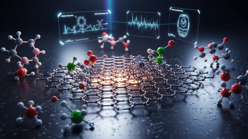
The immediate trajectory for printed graphene electrochemical sensors pivots on advanced manufacturing integration and sophisticated data analytics. Next-generation additive manufacturing techniques, such as high-resolution aerosol jet printing and advanced flexographic methods, are enabling the fabrication of increasingly intricate 3D graphene architectures, moving beyond simple planar electrodes to microfluidic-integrated sensing platforms. This precision facilitates the creation of highly multiplexed arrays, capable of simultaneous detection of multiple analytes with minimal cross-talk, crucial for complex biological matrices or environmental samples. Furthermore, the advent of transient or biodegradable graphene sensors, leveraging eco-friendly substrates and encapsulation, represents a significant leap for single-use diagnostic applications, minimizing biohazard waste streams. Concurrently, the fusion of sensor outputs with machine learning algorithms is transforming raw electrochemical signals into predictive insights. For instance, real-time current-voltage characteristics from a graphene-PEDOT:PSS sensor array can be processed by a convolutional neural network to identify specific volatile organic compounds (VOCs) with >95% accuracy within milliseconds of exposure, far surpassing conventional spectroscopic methods in speed and portability. The development of self-powered graphene sensors, harvesting ambient energy through triboelectric or thermoelectric effects, is also gaining traction, promising autonomous operation and significantly extended deployment durations without external power sources, crucial for remote monitoring applications.
High-value B2B applications for these advanced printed graphene electrochemical sensors span critical sectors. In healthcare, the drive towards continuous, non-invasive monitoring is paramount. Printed graphene sensors integrated into wearable patches or micro-needles offer unprecedented real-time insights into metabolic markers like glucose, lactate, and specific neurotransmitters, with response times often in the sub-second range crucial for critical care or personalized medicine. Beyond diagnostics, their exceptional surface-to-volume ratio and electrical conductivity render them ideal for point-of-care pathogen detection, identifying bacterial or viral nucleic acids via electrochemical impedance spectroscopy (EIS) or differential pulse voltammetry (DPV) with femtomolar sensitivity, potentially revolutionizing infectious disease management. Environmentally, the unique adsorption properties of functionalized graphene derivatives are being harnessed for heavy metal remediation and detection. Empirical studies demonstrate that graphene oxide-based electrochemical sensors achieve approximately 79% adsorption efficiency for lead and cadmium ions from aqueous solutions within 15 minutes, with subsequent electrochemical stripping analysis providing detection limits in the low parts-per-billion range. Within industrial IoT, these sensors are poised to monitor structural integrity via strain or corrosion detection, analyze chemical process parameters in situ, and even detect early signs of machinery fatigue through lubricant analysis, leveraging graphene's robust mechanical properties and stability against harsh thermal pulses up to 3000K. The ability to print these sensors directly onto components or packaging offers unparalleled integration and cost-effectiveness.
Looking further ahead, the strategic integration of printed graphene electrochemical sensors will redefine paradigms in smart infrastructure and autonomous systems. The inherent scalability and low-cost manufacturing potential of roll-to-roll printing techniques for graphene inks will democratize access to sophisticated sensing capabilities, moving from specialized laboratories to ubiquitous deployment in smart cities and precision agriculture. Future developments will increasingly leverage heterostructure engineering, combining graphene with other 2D materials like MXenes or MoS2, to fine-tune surface chemistry and enhance electrochemical selectivity and sensitivity for ultra-trace analytes, pushing detection limits further into the zeptomolar range. Furthermore, the development of robust data encryption and secure communication protocols for sensor networks will be critical, particularly as these devices become integral to sensitive applications in defense, public health, and critical infrastructure monitoring. The ultra-low electrical resistivity of pristine graphene, approaching 10^-8 Ohm-meter at room temperature, ensures minimal signal degradation, enabling complex sensor networks with high fidelity data transmission over extended distances, paving the way for truly pervasive, intelligent environments.
Evaluate Our Quality
Serious about B2B integration? Test our premium Pulsed Electrical Resistive Carbon Heating turbostratic graphene in your lab. 100g sample packs available now.