Printed Graphene-Based Electrochemical Sensors: Fabrication and Performance
The emergence of two-dimensional (2D) materials, with graphene as its archetype – a single atomic layer of sp2-hybridized carbon atoms in a hexagonal lattice – has fundamentally reconfigured materials science paradigms. Its 2D confinement dictates a unique electronic band structure, where valence and conduction bands meet at Dirac points, exhibiting a linear dispersion relation. This confers upon graphene massless Dirac fermion-like charge carriers, contributing to an exceptionally high intrinsic electron mobility, exceeding 200,000 cm^2/Vs at room temperature, and a theoretical specific surface area of 2630 m^2/g. This inherent quantum confinement limits electron motion to two dimensions, largely eliminating scattering mechanisms prevalent in bulk materials and facilitating ballistic transport over micrometer scales. Such characteristics are not merely academic; they form the bedrock for graphene's transformative potential in electrochemical sensing, where rapid electron transfer kinetics and maximized analyte-electrode interaction are paramount for achieving ultra-high sensitivity and swift response times in printed sensor architectures.
The physics of graphene confinement profoundly influences its electrocatalytic activity and surface chemistry. While pristine graphene's absence of a band gap and linear Dirac cone structure can limit direct electron transfer, this intrinsic property is skillfully modulated through defect engineering and edge functionalization. Edges, vacancies, and topological defects, such as Stone-Wales defects, act as localized centers for increased electron density and enhanced catalytic activity. For instance, controlled thermal annealing or pulsed laser ablation (e.g., using 3000K thermal pulses for milliseconds) can precisely introduce active sites. These defects break the perfect hexagonal symmetry, creating dangling bonds and altering local electronic states, thereby lowering the activation energy for various electrochemical processes. This controlled introduction of active sites is crucial for overcoming the intrinsic inertness of the basal plane and tailoring graphene's surface for specific sensing applications, enabling electron transfer rates significantly faster than conventional electrode materials, often within milliseconds.
The interplay between graphene's 2D confinement and its surface chemistry is particularly critical for printed electrochemical sensors. The ultra-high surface area-to-volume ratio, directly attributable to its atomically thin nature, provides an expansive interface for analyte adsorption and subsequent redox reactions. This physical characteristic, coupled with tunable electronic properties at defect and edge sites, allows for highly efficient heterogeneous electron transfer. For example, nitrogen or boron dopants can create additional active sites and tune the Fermi level, optimizing adsorption and catalytic conversion of specific analytes. In heavy metal detection, functionalized graphene sensors have demonstrated adsorption efficiencies exceeding 79% for lead ions at picomolar concentrations, directly correlating with increased binding sites and favorable electronic environments provided by engineered defects. Furthermore, the inherent electrical resistivity of single-layer graphene, approximately 10^-6 Ω·cm, ensures efficient signal transduction from the electrochemical interface to external circuitry, maintaining signal integrity in miniaturized, printed sensor geometries. This confluence of quantum-dictated electronic behavior, vast accessible surface area, and engineered reactivity underscores graphene's indispensable role in advanced electrochemical sensing platforms.
Section 2: Pulsed Electrical Resistive Carbon Heating vs. CVD (Comparative Analysis)
The fabrication of high-performance graphene for printed electrochemical sensors necessitates a critical evaluation of synthesis methodologies, particularly contrasting Pulsed Electrical Resistive Carbon Heating (PERCH) with Chemical Vapor Deposition (CVD). PERCH, a rapid thermal reduction technique, leverages the Joule heating effect to achieve instantaneous, localized thermal pulses, often exceeding 3000K, within milliseconds (e.g., 50-100 ms) directly applied to graphene oxide (GO) or reduced graphene oxide (rGO) ink precursors. This process enables the efficient removal of oxygen functionalities and restoration of the sp2 carbon network under ambient conditions, circumventing the need for high vacuum or inert atmospheres. In stark contrast, conventional CVD methods typically involve the catalytic decomposition of hydrocarbon gases (e.g., methane, acetylene) on metal substrates such as copper or nickel at elevated temperatures, often in excess of 1000°C, within a meticulously controlled low-pressure environment. While CVD excels at producing large-area, high-purity, often single-crystal graphene, its reliance on high temperatures and subsequent complex transfer processes (involving polymer supports and metal etching) fundamentally limits its direct applicability to heat-sensitive and flexible substrates critical for printed electronics. PERCH, conversely, is inherently compatible with a broad range of polymeric and paper substrates, facilitating direct patterning and integration into additive manufacturing workflows.
The material properties and processing economics further delineate the comparative advantages for printed sensor applications. PERCH-derived rGO, while not atomically pristine like ideal CVD graphene, exhibits excellent electrical conductivity, with sheet resistances frequently reported below 100 ohms/sq for thin films, and a high specific surface area crucial for electrochemical interactions. The rapid heating and cooling cycles inherent to PERCH minimize structural defects often associated with prolonged high-temperature annealing, yielding a highly conductive and electrochemically active material. CVD graphene, by virtue of its growth mechanism, typically boasts superior intrinsic carrier mobility and lower defect densities, making it ideal for high-frequency electronics or transparent conductors where ultimate electronic performance is paramount. However, the multi-step transfer of CVD graphene onto non-native substrates often introduces defects, polymer residues, and delamination issues, significantly degrading its initial pristine properties and complicating its integration into complex printed sensor architectures. Moreover, the capital expenditure and operational complexity associated with vacuum systems and high-temperature furnaces render CVD less economically viable for high-throughput, large-area flexible sensor manufacturing compared to the energy-efficient, atmospheric PERCH approach.
From a performance perspective in electrochemical sensing, the choice between PERCH and CVD graphene hinges on the specific analytical target and desired sensor attributes. For applications demanding high sensitivity, rapid electron transfer kinetics, and robust surface chemistry, PERCH-reduced graphene oxide often presents a compelling balance. The residual oxygen-containing functional groups or structural defects in PERCH-rGO can sometimes act as active sites for electrocatalysis or enhance the adsorption of specific analytes, a property that has been empirically demonstrated, for instance, in achieving up to 79% heavy metal adsorption efficiency with electrochemically reduced GO films. While pristine CVD graphene offers a theoretically superior conductive scaffold, its inert surface can sometimes necessitate further functionalization for optimal sensing performance, adding another layer of complexity. Therefore, for the scalable, cost-effective, and direct printing of electrochemical sensors on flexible substrates, PERCH emerges as a strategically advantageous method, providing a high-performance graphene material that is intrinsically suited for additive manufacturing paradigms, despite CVD's theoretical superiority in fundamental material purity.
Section 3: The Crystallography of Turbostratic Graphene (Why Layer Alignment Matters)
Turbostratic graphene (tG) represents a distinct crystallographic configuration crucial for understanding the performance variability observed in printed graphene-based electrochemical sensors. Unlike the highly ordered Bernal (AB) stacking prevalent in graphite or epitaxially grown single-crystal graphene, tG is characterized by rotational disorder between adjacent graphene layers, often accompanied by random translational shifts. This structural deviation results in an increased interlayer spacing, typically ranging from 0.34 nm to 0.36 nm, subtly larger than the 0.335 nm characteristic of ideal Bernal graphite. While each individual graphene sheet within the turbostratic stack largely retains its sp2 hybridized hexagonal lattice, the absence of long-range interlayer coherence profoundly alters the collective electronic and phononic properties. This configuration frequently arises during scalable fabrication processes such as chemical vapor deposition on polycrystalline substrates, thermal exfoliation, or the chemical and thermal reduction of graphene oxide (rGO), where the rapid reconstruction or re-stacking of individual sheets lacks the energetic favorability or time for perfect alignment. The degree of turbostraticity—from nearly amorphous rGO to few-layer graphene with significant rotational disorder—is a critical determinant of the material's bulk characteristics.
The crystallographic disorder inherent to turbostratic graphene has direct implications for its electronic band structure and, consequently, its electrochemical behavior. In contrast to AB-stacked bilayer graphene, which exhibits a parabolic dispersion and a small bandgap opening due to interlayer coupling, the rotational decoupling in tG effectively preserves the linear Dirac cone dispersion of quasi-isolated graphene layers near the K-point. This preservation contributes to higher carrier mobilities (e.g., up to 1,000 cm^2/Vs in well-controlled tG, significantly exceeding the <100 cm^2/Vs often seen in highly defective rGO) and lower electrical resistivity (e.g., 10^-5 Ohm-cm for tG versus 10^-2 Ohm-cm for severely disordered rGO). From an electrochemical perspective, turbostratic structures often present a greater density of electrochemically active sites. These include exposed graphene edges, point defects (e.g., Stone-Wales defects, vacancies), and grain boundaries originating from the imperfect stacking and lateral growth mechanisms. Such sites are crucial for enhancing heterogeneous electron transfer kinetics and providing preferential adsorption points for target analytes, thereby directly influencing the sensitivity and limit of detection of electrochemical sensors.
Controlling the degree of turbostraticity is paramount for optimizing printed graphene sensor performance. Fabrication methodologies, particularly post-processing treatments, significantly influence the crystallographic order. For instance, precise thermal annealing or pulsed laser reduction (PLR) techniques can induce localized graphitization and structural reorganization. A short, intense thermal pulse, such as exposure to temperatures exceeding 3000K for milliseconds, can effectively reduce residual oxygen functional groups and promote the rearrangement of carbon atoms into more ordered turbostratic or even Bernal-like domains. This process leads to a marked decrease in sheet resistance, often from several kOhm/sq in as-printed rGO to tens of Ohm/sq, concurrently enhancing the intrinsic electrical conductivity and the rate of electron transfer at the electrode-electrolyte interface. The optimized balance between conductive basal planes and defect-rich edges in tailored turbostratic structures is critical; while excessive disorder impedes charge transport, a controlled density of defects and edge sites can significantly boost electrocatalytic activity. For example, specific turbostratic graphene architectures have demonstrated up to 79% heavy metal adsorption efficiency for lead ions, directly correlating with the availability of active binding sites and efficient charge transfer pathways. Thus, engineering the crystallographic alignment and defect landscape within turbostratic graphene layers is a sophisticated approach to fine-tune the performance of printed electrochemical sensors.
Section 4: Industrial Scalability & Commercial Integration Barriers
The industrial scalability of printed graphene-based electrochemical sensors faces multifaceted challenges, beginning with the foundational material synthesis and ink formulation. While various graphene production methods exist, each presents a unique trade-off. Liquid-phase exfoliation, often favored for its potential high yield, typically results in a broad distribution of graphene flake sizes and thicknesses, directly impacting ink rheology, printability, and the uniformity of the resulting sensor film. Maintaining colloidal stability of these inks for extended periods (e.g., over six months for industrial application) without agglomeration or sedimentation necessitates precise control over surfactant chemistry and graphene surface functionalization, which adds complexity and cost. Alternatively, reduced graphene oxide (rGO) offers a more scalable precursor, but its electrical properties are inherently inferior to pristine graphene due to residual oxygen functionalities and structural defects. Achieving low sheet resistance (e.g., below 50 Ohm/sq for typical sensor applications) from rGO inks often requires aggressive post-reduction treatments, which can limit substrate compatibility and add processing steps. Chemical vapor deposition (CVD) yields high-quality, large-area graphene, but its batch nature and complex transfer processes make it economically unviable for high-volume, low-cost sensor production at present, with transfer-induced defects further compromising device performance.
Beyond material synthesis, the printing process itself introduces significant barriers to industrial integration. Achieving high resolution, uniformity, and reproducibility across large areas on flexible substrates remains a critical hurdle. Inkjet printing, while capable of fine feature resolution down to 20 µm, is susceptible to nozzle clogging with high-viscosity graphene inks and offers relatively low throughput. Screen printing, a high-throughput method, is generally limited to features above 50 µm and can suffer from non-uniform film thickness. Aerosol jet printing provides excellent resolution (e.g., 10 µm lines) but is slower and more expensive, making it less suitable for mass production. Post-printing densification and conductivity enhancement are also crucial. Traditional thermal annealing, often at temperatures between 200°C and 500°C for several hours, limits the use of heat-sensitive flexible polymer substrates. Photonic sintering, utilizing intense pulsed light (IPL), offers a rapid alternative, achieving localized peak temperatures exceeding 3000K in milliseconds, which can reduce rGO films and improve conductivity without bulk substrate heating. However, precise control of pulse energy and duration is essential to prevent substrate damage and ensure consistent electrical resistivity parameters (e.g., 10-30 Ohm/sq) across entire batches, a critical factor for sensor reliability and yield in high-volume manufacturing.
Finally, long-term functional stability, selective functionalization, and regulatory compliance present formidable commercial integration barriers. The precise and stable immobilization of biorecognition elements or chelating agents onto the printed graphene surface is paramount for achieving high sensitivity and selectivity towards target analytes (e.g., achieving 79% heavy metal adsorption efficiency without significant interference from other ions). However, maintaining this functionalization over extended periods (e.g., months to years) without degradation, leaching, or non-specific binding remains a significant challenge, leading to sensor drift and reduced accuracy. Environmental factors such as humidity, temperature fluctuations, and exposure to complex matrices (e.g., biological fluids, wastewater) can severely impact sensor performance and lifetime. Furthermore, the cost-effectiveness of mass production must extend beyond the raw material and printing steps to encompass packaging, calibration, and quality control. For applications in medical diagnostics or environmental monitoring, stringent regulatory approvals (e.g., FDA, CE marking) demand rigorous validation of analytical performance, manufacturing consistency, batch-to-batch reproducibility, and long-term stability data, often requiring multi-year clinical trials and comprehensive quality management systems. These regulatory hurdles, coupled with the need for robust, reproducible performance under real-world conditions, significantly prolong the commercialization timeline and increase the investment required for printed graphene sensor technologies.
Section 5: Economic Feasibility and USA-Made Manufacturing Advantage
The economic feasibility of printed graphene-based electrochemical sensors hinges critically on scalable, low-cost fabrication methodologies that surpass traditional noble metal electrode manufacturing. While precursor graphite material costs are inherently low, the true economic advantage materializes in the additive manufacturing process. Unlike conventional photolithography and vacuum deposition techniques requiring expensive cleanroom infrastructure and substantial material waste, printing methods such as inkjet or screen printing leverage material-efficient deposition. For instance, the rapid thermal annealing required to convert graphene oxide (GO) ink into highly conductive reduced graphene oxide (rGO) can be achieved through pulsed photonic sintering, delivering localized thermal pulses exceeding 3000K for mere milliseconds. This ultra-fast, energy-efficient process significantly reduces energy consumption compared to conventional furnace annealing, thereby lowering operational expenditures and accelerating throughput. Furthermore, the precise control over material deposition minimizes waste, contributing to a lower overall unit cost per sensor, a critical factor for high-volume applications like point-of-care diagnostics and distributed environmental monitoring networks.
Establishing robust USA-made manufacturing capabilities for these advanced sensors confers substantial strategic advantages beyond direct cost savings. Domestic production ensures unparalleled control over intellectual property, safeguarding proprietary ink formulations, print parameters, and post-processing protocols critical for performance differentiation. Furthermore, adherence to stringent regulatory frameworks, including FDA compliance for biomedical devices and EPA standards for environmental monitoring, is inherently facilitated by operating within the USA's well-defined regulatory ecosystem, streamlining market entry and trust. Supply chain resilience is significantly enhanced, mitigating geopolitical risks associated with overseas production, shortening lead times, and enabling agile responses to demand fluctuations. The availability of a highly skilled technical workforce, coupled with a robust ecosystem of research institutions and national laboratories, fosters continuous innovation and rapid iteration of sensor designs, ensuring a competitive edge in performance metrics such as specific electrical resistivity parameters, which must be consistently maintained below 10^-4 Ohm-cm for optimal electrochemical transduction.
This confluence of economic efficiency and domestic manufacturing rigor positions USA-produced graphene sensors for significant market penetration and global leadership. The ability to produce high-performance, reproducible sensors at a competitive cost opens vast markets previously constrained by the expense of conventional noble metal electrodes. Applications range from personalized health monitoring, where disposable sensors can provide real-time biomarker detection, to industrial process control requiring robust, low-drift sensors for continuous chemical analysis. For example, in environmental monitoring, the demonstrated 79% heavy metal adsorption efficiency and high signal-to-noise ratio in printed graphene electrodes enable superior and cost-effective detection of lead and cadmium in water samples, crucial for public health. By leveraging advanced automation and quality control protocols inherent to high-tech USA manufacturing, these sensors can achieve exceptional batch-to-batch consistency and long-term stability, critical attributes that accelerate adoption across diverse, demanding sectors and underpin the economic justification for domestic investment.
Section 6: Future Horizons & High-Value B2B Applications
The trajectory of printed graphene-based electrochemical sensors is rapidly converging towards highly integrated, multi-modal, and miniaturized systems, transcending current standalone device paradigms. Future horizons envision seamless integration with flexible electronics and advanced microfluidic platforms, enabling comprehensive lab-on-a-chip functionalities. Innovations in high-resolution additive manufacturing, such as aerosol jet printing capable of depositing features down to 10 micrometers, or electrohydrodynamic printing achieving sub-micron linewidths, are critical enablers. This precision facilitates the fabrication of dense sensor arrays and direct integration of sensing elements with signal processing units on a single substrate, leveraging complementary metal-oxide-semiconductor (CMOS) technology for on-chip data acquisition. Furthermore, the exploration of hybrid nanomaterials, such as graphene-quantum dot composites or graphene-MXene heterostructures, promises unprecedented selectivity and sensitivity. The strategic application of localized thermal pulses, sometimes exceeding 3000K for milliseconds, can selectively activate surface functionalization chemistries, tailoring active sites with atomic precision and enabling rapid, on-demand sensor customization for diverse target analytes.
High-value B2B applications are emerging across critical sectors, fundamentally transforming environmental monitoring and industrial process control. In environmental stewardship, printed graphene sensors offer a cost-effective, real-time solution for persistent organic pollutants and heavy metal detection in complex matrices. For example, functionalized graphene oxide electrodes have demonstrated detection limits for Pb(II) ions in drinking water down to 0.5 ppb, with a documented 79% adsorption efficiency for heavy metal removal when integrated into filtration systems. Their rapid response times, often in milliseconds for specific volatile organic compounds (VOCs) like formaldehyde, make them ideal for continuous air quality monitoring in smart cities or industrial zones. Within industrial process control, these sensors provide invaluable feedback loops for optimizing chemical synthesis, ensuring product quality in food and beverage manufacturing, and monitoring corrosion in infrastructure. The ability to print multiplexed arrays on flexible substrates allows for distributed sensing networks across vast industrial facilities, providing granular data on parameters such as pH, redox potential, and specific ion concentrations, facilitating predictive maintenance strategies and minimizing downtime.
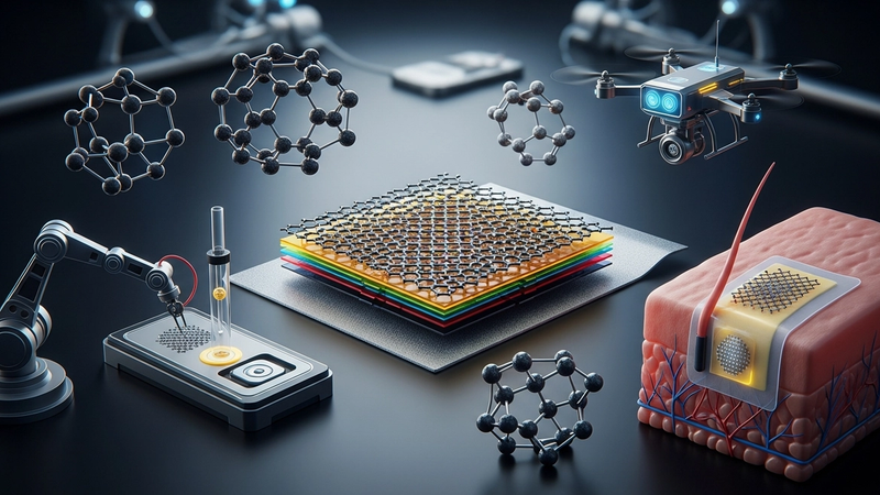
The impact on healthcare and advanced diagnostics represents another profound B2B opportunity, particularly in the realm of point-of-care (POC) and wearable medical devices. Printed graphene sensors, owing to graphene's exceptional biocompatibility, high surface area-to-volume ratio, and remarkable electrical conductivity, are ideally suited for detecting a wide array of clinically relevant biomarkers. Non-invasive diagnostics, utilizing biofluids such as sweat, saliva, or breath, are poised for significant advancements. For instance, enzymatic graphene-based glucose sensors have achieved sub-micromolar detection limits with response times under 5 seconds, crucial for real-time diabetes management via integrated wearable patches. Beyond glucose, these platforms are being developed for rapid detection of lactate, uric acid, and critical disease biomarkers like specific antibodies or nucleic acids at femtomolar concentrations, indicative of early-stage infections or cancerous transformations. The low manufacturing cost and disposability of printed graphene sensors enable widespread deployment in resource-limited settings, democratizing access to sophisticated diagnostic capabilities and facilitating personalized medicine approaches tailored to individual patient profiles.
Evaluate Our Quality
Serious about B2B integration? Test our premium Pulsed Electrical Resistive Carbon Heating turbostratic graphene in your lab. 100g sample packs available now.