Optimizing Graphene Thermal Contacts for Nanoelectronics
Graphene, the revolutionary two-dimensional material, continues to capture the imagination of scientists and engineers worldwide. Its extraordinary properties, especially its exceptional thermal conductivity, position it as a game-changer for next-generation micro- and nanoelectronics. However, translating graphene's inherent advantages into practical applications is not without its hurdles. One of the most fundamental challenges lies in establishing high-quality electrical and thermal contacts between graphene and conventional metal electrodes.
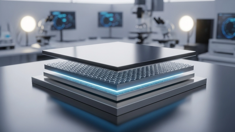
The efficiency of heat dissipation and electrical transport in graphene-based devices hinges critically on these interfaces. Poor contact quality can severely diminish graphene's performance, hindering its potential for advanced heat management solutions. Addressing this crucial issue requires innovative approaches to interface engineering.
Recent advancements in annealing techniques, particularly nonlocal laser annealing, are offering promising pathways to overcome these limitations. By precisely manipulating the interface at a microscopic level, researchers are achieving significant improvements in graphene thermal contacts, paving the way for more reliable and higher-performing graphene-enabled technologies. This exploration delves into the science behind these contact improvements, the methods employed for characterization, and the implications for the future of nanoelectronics.
The Critical Challenge of Graphene-Metal Interfaces in Nanoelectronics
The integration of graphene into functional electronic devices inherently requires robust interfaces with metallic electrodes. These contacts serve dual roles: facilitating efficient electrical transport and, perhaps even more critically, enabling effective heat dissipation. In the sub-micrometer scale of modern nanoelectronics, where heat generation is often localized and intense, the ability to rapidly transfer thermal energy away from active components is paramount for device stability and longevity.
Despite graphene's unparalleled intrinsic thermal conductivity, its full potential in heat management applications can be severely compromised by suboptimal thermal contacts. This issue manifests as a bottleneck at the interface, impeding the efficient flow of heat from the graphene layer into the broader heat sink provided by the metal electrode. Consequently, even with highly conductive graphene, localized hotspots can develop, leading to performance degradation and premature device failure.
Moreover, the formation of high-quality graphene-metal thermal contacts is a complex endeavor. The atomic-scale precision required for ideal bonding often conflicts with the practicalities of large-scale manufacturing and the inherent surface roughness of typical metal electrodes. While theoretical studies on graphene-metal contacts are abundant, experimental investigations into their thermal properties remain comparatively scarce, highlighting a significant gap in our understanding and development capabilities.
Researchers are actively exploring various methodologies to bridge this gap, recognizing that the quality of these interfaces is as crucial as the intrinsic properties of the graphene itself. The goal is not just to establish a connection, but to create an interface that maximizes the transfer efficiency for both charge carriers and thermal energy, thereby unlocking the true potential of graphene in high-performance nanoelectronic systems.
Unlocking Enhanced Graphene Thermal Contacts Through Advanced Annealing
Addressing the fundamental challenge of poor graphene-metal interfaces necessitates innovative processing techniques. Among the most promising methods for significantly enhancing the quality of both electrical and thermal contacts is advanced annealing, with nonlocal laser annealing emerging as a particularly effective strategy. This technique leverages precisely controlled laser energy to induce localized modifications at the graphene-metal junction, thereby improving critical contact properties.
The core mechanism behind the improvement of thermal contacts, especially between few-layer graphene (FLG) or multilayer graphene (MLG) and initially rough metal electrodes, is attributed to the local melting of the metal surface under intense laser heating. When the laser energy is absorbed, the localized temperature rise at the interface can momentarily exceed the melting point of the metal. This transient melting allows the metal surface to flow and conform more intimately with the graphene flakes, effectively increasing the real contact area between the two materials.
An increased real contact area is paramount for efficient heat transfer. Thermal energy typically propagates across interfaces through phonons, and a larger, more intimate interface facilitates a greater number of phonon coupling pathways. This enhanced coupling leads to a reduction in thermal contact resistance, allowing heat to dissipate more effectively from the graphene layer into the metal heat sink. The power of the laser is a critical parameter, as increased laser power was specifically shown to result in significantly decreased local temperature of graphene under subsequent laser heating, directly indicating improved thermal conduction.
While conventional annealing methods can also offer some improvements, nonlocal laser annealing provides distinct advantages. Its localized nature allows for precise targeting of specific contact regions without affecting surrounding sensitive device components. Furthermore, the rapid heating and cooling cycles inherent to laser processing can create unique microstructures at the interface that are beneficial for contact formation. This ability to precisely engineer the interface at a micro- or nanoscale underscores the transformative potential of laser annealing in optimizing graphene thermal contacts for high-performance nanoelectronic applications.
Precision Measurement: The Role of Micro-Raman Spectroscopy in Contact Characterization
Accurately quantifying the improvements in graphene thermal contacts and thermal conductivity requires sophisticated measurement techniques. Among these, the opto-thermal micro-Raman method stands out as a powerful and versatile tool, particularly for suspended few-layer graphene (FLG) and multilayer graphene (MLG) flakes. This technique offers a non-contact, high-resolution approach to determine local temperature and, by extension, thermal properties.
The micro-Raman technique operates by analyzing the shifts in specific Raman peaks of graphene, which are highly sensitive to temperature changes. By applying laser heating to a suspended graphene flake and simultaneously monitoring its Raman spectrum, researchers can deduce the local temperature rise. Knowing the input laser power and the geometry of the system, the thermal conductivity of the graphene and the thermal contact resistance at its interfaces can be calculated.
However, the accuracy of these thermal conductivity measurements depends critically on the quality of the thermal contacts between the graphene flakes and the metal electrodes, which typically serve as heat sinks. If the contacts are poor, a significant portion of the heat generated by the laser will not efficiently transfer into the electrodes, leading to an overestimation of the graphene's local temperature and, consequently, an inaccurate determination of its thermal conductivity. This highlights a crucial feedback loop: the very contacts we are trying to improve are essential for accurately measuring the improvement.
For experimental studies of thermal contacts between FLG and MLG, the confocal micro-Raman method at low laser power is employed. This allows for precise measurements without inducing significant alterations to the contact itself. Subsequently, by applying increased laser power during the annealing process, the formation of improved thermal contacts can be directly observed through a measurable decrease in the local graphene temperature. This real-time, in-situ observation capability makes micro-Raman an indispensable tool for both characterizing and optimizing graphene thermal contacts.
Other methods such as the thermal bridge and four-point probe techniques also exist for measuring thermal conductivity, often relying on indirect optical or electrical means for heating and local temperature measurements. However, the direct spectroscopic temperature sensitivity and spatial resolution of micro-Raman make it particularly well-suited for detailed investigations of the thermal interfaces critical for advanced graphene devices.
From Graphite to High-Performance Graphene: Fabrication and Deposition Techniques
The journey to achieving high-performance graphene-based devices begins with the meticulous preparation and precise deposition of graphene flakes. While various methods exist for fabricating single-layer graphene (SLG), few-layer graphene (FLG), and multilayer graphene (MLG), the choice of technique profoundly impacts the material's quality and its suitability for specific applications, particularly when it comes to forming robust contacts.
Among the array of preparation methods, which include chemical vapor deposition (CVD), super-short-pulse laser produced plasma deposition, reduction of graphene oxide, exfoliation through thermal shock, and acid treatment of expandable graphite, the conventional low-cost liquid-phase exfoliation method stands out for producing freestanding graphene flakes. This technique is particularly valuable for research focusing on thermal contacts, as it yields graphene that largely retains the quality of its initial bulk graphite source, a crucial factor for exhibiting intrinsic thermal properties.
In this specific research context, natural graphite powder served as the starting material. The liquid-phase exfoliation process involved sonicating the graphite in suitable solvents, such as N,N-dimethylformamide (DMF) or isopropyl alcohol (IPA). The effectiveness of this exfoliation relies on a critical principle: the surface energy of the solvent and the solute (graphene) must be closely matched. For instance, the Hildebrand solubility parameters for DMF (24.86 MPa^1/2), IPA (23.58 MPa^1/2), and graphene (~23 MPa^1/2) are indeed very close, facilitating efficient exfoliation.
Sonication, which generates shock waves and microjets in the liquid, mechanically delaminates the graphite layers. Following sonication, centrifugation is employed to separate the exfoliated graphene flakes from unexfoliated graphite. The supernatant solution, rich in high-quality FLG and MLG flakes, with lateral sizes ranging from 0.5 to 10 µm and impressive lateral size-to-thickness ratios of up to 200–300, is then carefully collected for subsequent use and analysis.
Once prepared, these graphene flakes must be precisely positioned onto metallic electrodes to form the desired device structures. For this, the AC di-electrophoresis technique is employed. This method uses an alternating current electric field to manipulate and deposit the graphene flakes from the dispersion onto pre-patterned metallic electrodes. This controlled deposition is essential for creating the well-defined interfaces necessary for studying and optimizing graphene thermal contacts, ensuring that the flakes are accurately placed for subsequent annealing and characterization processes.
Beyond Metal: Understanding Heat Transfer in Graphene-Based Systems
While the focus on graphene-metal contacts is crucial for electronic device integration, understanding heat transfer in graphene extends beyond these interfaces to other relevant substrates. The extraordinary thermal properties of graphene make it highly attractive for heat management in various micro- and nanoelectronics contexts, motivating numerous studies into its diverse applications. However, the efficiency of heat dissipation can vary significantly depending on the material graphene is coupled with.
Intriguingly, observations indicate that the improvement of thermal contacts is not exclusive to graphene-metal interfaces. Similar enhancements were also observed between multilayer graphene (MLG) and silicon oxide surfaces. More importantly, the research highlighted that heat transfer from graphene to a silicon oxide surface can be even more efficient compared to the graphene-metal case. This finding has significant implications, suggesting that the choice of substrate or encapsulation material plays a critical role in the overall thermal performance of graphene-based systems.
The superior heat transfer to silicon oxide might be attributed to different interfacial phonon coupling mechanisms, cleaner interfaces, or optimized surface energy matching that allows for a more intimate contact than typically achieved with rough metal surfaces. This understanding opens new avenues for device design, where strategic selection of dielectric layers could further enhance the thermal performance of graphene. It underscores that heat management in graphene is a multifaceted problem, demanding a holistic approach that considers not only the graphene's intrinsic conductivity but also the thermal characteristics of all adjacent materials.
Ultimately, for successful applications in heat management, two factors are equally important: the inherently high thermal conductivity of graphene itself and the equally high quality of its thermal contacts with surrounding materials, whether they are metals for electrodes or dielectrics for substrates and passivation layers. The interplay between these factors dictates the overall thermal resistance of a device and its ability to dissipate heat effectively. Future research will undoubtedly continue to explore these varied interfaces, aiming to engineer optimal heat transfer pathways that fully leverage graphene's unique thermal attributes across a wide range of nanoelectronic architectures.
Conclusion: Paving the Way for Future Graphene Nanoelectronics
The journey to fully harness graphene's extraordinary properties for advanced nanoelectronics is fundamentally linked to our ability to create and maintain high-quality interfaces. The challenge of poor electrical and thermal contacts between graphene and metal electrodes has long been a bottleneck, impacting the efficiency of both charge transport and, crucially, heat dissipation in sub-micrometer scale devices. However, the insights gained from studies into advanced annealing techniques offer a clear path forward.
Nonlocal laser annealing, by inducing localized melting and increasing the real contact area, stands out as a powerful method to significantly enhance graphene thermal contacts. Coupled with the precision of micro-Raman spectroscopy for accurate characterization, this approach allows for the systematic optimization of these critical interfaces. The understanding derived from these studies not only improves graphene-metal contacts but also sheds light on the broader principles of heat transfer in graphene-based systems, including the surprisingly efficient coupling with silicon oxide.
As the demand for smaller, faster, and more powerful electronic devices continues to grow, effective heat management becomes increasingly vital. The advancements in optimizing graphene thermal contacts are not merely incremental improvements; they represent a fundamental step towards unlocking the full potential of few-layer and multilayer graphene in next-generation thermal management solutions. These high-quality contacts, combined with graphene's exceptional thermal conductivity, are poised to transform the landscape of micro- and nanoelectronics.
Are you ready to integrate the power of optimized graphene into your next-generation applications? Explore the possibilities and discover high-quality graphene materials designed for demanding thermal and electrical performance. Visit usa-graphene.com today to learn more about our innovative graphene solutions and how we can support your advanced research and development needs.
Evaluate Our Quality
Serious about B2B integration? Test our premium Pulsed Electrical Resistive Carbon Heating turbostratic graphene in your lab. 100g sample packs available now.