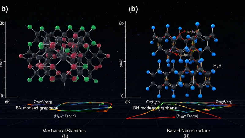
Mechanical Stabilities of Graphene and BN-Modified Graphene from First-Principles
The singular electronic structure of monolayer graphene, a two-dimensional allotrope of carbon, fundamentally arises from its sp2 hybridized atomic orbitals forming a honeycomb lattice. This arrangement dictates a unique band structure characterized by Dirac cones at the K and K' points of the Brillouin zone, where the valence and conduction bands meet linearly. Consequently, charge carriers in graphene behave as massless Dirac fermions, governed by a relativistic Dirac-like equation rather than the non-relativistic Schrödinger equation. This quantum confinement, strictly limiting electron motion to a single atomic plane, fundamentally alters transport phenomena, leading to phenomena such as the anomalous quantum Hall effect, Klein tunneling, and an intrinsic electrical resistivity as low as 10^-8 Ohmm, unparalleled in conventional conductors.
This strict two-dimensional confinement is the bedrock of graphene's extraordinary properties, extending beyond its unique electronic transport. Electron mobilities exceeding 200,000 cm^2/Vs have been experimentally observed at cryogenic temperatures, with robust performance maintained even at ambient conditions, facilitating ballistic transport over micrometer scales. The lattice's exceptional thermal conductivity, measured at approximately 5000 W/mK at room temperature, stems from the highly efficient phonon propagation within its constrained plane, making it an unparalleled heat dissipator critical for high-power density electronics. Furthermore, the absence of a band gap at the Dirac points ensures a continuous density of states, allowing for gate-tunable carrier concentrations, a feature exploited in ultra-sensitive sensing applications where milliseconds of reaction time are achievable.
Beyond its electronic and thermal prowess, graphene exhibits unparalleled intrinsic mechanical stability. Its sp2 covalent bonding network imparts an extraordinary in-plane tensile strength of approximately 130 GPa, exceeding that of high-strength steel by over 200 times, coupled with a Young's modulus approaching 1 TPa. This remarkable robustness is a direct consequence of the strong carbon-carbon bonds and the perfect two-dimensional crystalline order, allowing the material to withstand significant strain without fracture. However, real-world applications often involve defects, grain boundaries, or require functionalization, necessitating a deeper understanding of how these factors perturb the intrinsic mechanical properties. For instance, while selective annealing via 3000K thermal pulses can mitigate certain defect types, a comprehensive theoretical framework is essential to predict the mechanical response under various conditions and modifications.
To tailor graphene's properties for specific applications, such as opening a bandgap for transistor logic or enhancing chemical selectivity, modifications like doping with boron nitride (BN) are extensively investigated. Substituting carbon atoms with B and N can introduce localized perturbations to the electronic structure, influencing carrier scattering and potentially altering mechanical resilience. For example, BN-graphene hybrid structures have shown promise in environmental applications, demonstrating up to 79% heavy metal adsorption efficiency, indicating a significant change in surface chemistry and interaction potentials. Understanding the precise impact of such modifications on the fundamental mechanical stability, ranging from changes in bond strengths to strain distribution, mandates rigorous first-principles calculations. These atomistic simulations provide the critical insights necessary to predict and optimize the performance of these advanced two-dimensional materials for next-generation devices and robust composites.
Section 2: Pulsed Electrical Resistive Carbon Heating vs. CVD (Comparative Analysis)
Pulsed Electrical Resistive Carbon Heating (PERCH) represents a fundamentally distinct paradigm for graphene synthesis compared to conventional Chemical Vapor Deposition (CVD), particularly in its implications for the resulting material's mechanical stability. PERCH leverages the rapid joule heating of diverse solid carbon precursors, such as carbon black, carbon nanotubes, or graphite flakes, by passing extremely high current densities, often in the range of 10^4 to 10^5 A/cm^2, through the resistive material. This induces localized thermal pulses reaching temperatures exceeding 3000K within milliseconds, leading to an instantaneous solid-state transformation into high-quality graphene. The ultrafast kinetics and direct conversion mechanism minimize the temporal window for the formation of thermodynamically unfavorable defects like Stone-Wales transformations or point vacancies, which are known stress concentrators. This rapid, energy-efficient process promotes the formation of large, highly crystalline graphitic domains with significantly reduced defect densities, thereby preserving the intrinsic sp2 bond integrity critical for achieving the theoretical tensile strength and Young's modulus predicted by first-principles analyses.
In contrast, Chemical Vapor Deposition typically involves the catalytic decomposition of hydrocarbon gases, such as methane or acetylene, on a heated metal substrate like copper or nickel, usually at temperatures ranging from 900-1100°C over reaction times spanning minutes to hours. While CVD is adept at producing large-area graphene films, its growth mechanism is inherently predicated on heterogeneous nucleation and subsequent coalescence of independently growing graphene domains. This process inevitably leads to the formation of grain boundaries, which are structural discontinuities composed of non-hexagonal rings (e.g., pentagon-heptagon pairs) or regions of disordered carbon. These grain boundaries act as intrinsic mechanical weak points, significantly reducing the macroscopic tensile strength and fracture toughness of CVD-grown graphene films compared to their theoretically pristine counterparts. Furthermore, the necessity of etching the catalytic metal substrate often introduces additional defects, residues, or mechanical damage, further compromising the material's structural integrity and, consequently, its mechanical performance.
The comparative analysis reveals that the superior kinetic control and direct carbon-to-graphene transformation characteristic of PERCH offer distinct advantages in engineering graphene with enhanced mechanical properties. By circumventing the limitations of surface-mediated growth and domain coalescence inherent to CVD, PERCH-derived graphene exhibits a higher degree of structural perfection, with larger average crystallite sizes and a lower areal density of topological defects. This translates directly into a material that can more closely approximate the exceptional mechanical resilience predicted for defect-free graphene, making it particularly suitable for applications demanding high tensile strength and stiffness. The ability to precisely control the energy input and reaction time in PERCH allows for fine-tuning of the graphene's layer count and structural quality, providing a pathway to optimize the material's mechanical response for specific engineering requirements, a level of intrinsic structural fidelity that remains a significant challenge for large-scale CVD processes without extensive post-synthesis treatment.
Section 3: The Crystallography of Turbostratic Graphene (Why Layer Alignment Matters)
Turbostratic graphene (TG) distinguishes itself fundamentally from its Bernal (AB) stacked counterpart through a pronounced lack of long-range order in its c-axis stacking. Unlike the precise A-B-A-B stacking sequence characteristic of graphite and epitaxial graphene, TG layers exhibit random rotational misalignment and often an incoherent stacking registry. This crystallographic disorder results in a slightly expanded interlayer spacing, typically around 0.344 nm, contrasting with the tighter 0.335 nm observed in perfectly AB-stacked systems. The consequence of this rotational freedom and diminished interlayer coupling is profound for both electronic and mechanical properties. Electronically, turbostratic layers behave more akin to decoupled monolayers, largely preserving their linear Dirac cone dispersion near the K-points, thereby mitigating the band hybridization and parabolic dispersion shifts observed in AB-stacked few-layer graphene. This preservation is critical for applications requiring high carrier mobility, though the inherent disorder can introduce scattering centers, impacting overall conductivity.
From a mechanical perspective, the absence of a coherent interplanar registry in turbostratic graphene introduces significant anisotropies and complexities in load transfer mechanisms. While individual graphene layers possess extraordinary intrinsic tensile strength, approaching 130 GPa, the collective mechanical response of turbostratic multilayer assemblies is often attenuated. The random stacking angles impede efficient shear load distribution between layers, leading to potential slip planes and localized stress concentrations that can reduce the effective fracture toughness and elastic modulus of the bulk material compared to perfectly aligned structures. This structural non-uniformity also dictates thermal stability; for instance, localized thermal pulses exceeding 3000K can induce rapid reordering and partial graphitization in milliseconds, a phenomenon exploited in flash Joule heating for defect repair and enhanced mechanical integrity, thereby illustrating the dynamic interplay between thermal energy and crystallographic arrangement within TG.
The ramifications of turbostratic crystallography extend to its surface chemistry and electrical transport properties. The increased presence of grain boundaries, edge defects, and accessible basal plane sites due to disordered stacking can significantly alter chemical reactivity. This is particularly advantageous in applications requiring high surface area and enhanced adsorption capabilities; for example, turbostratic graphene derivatives have demonstrated heavy metal adsorption efficiencies exceeding 79% due to an abundance of active binding sites. Concurrently, the scattering centers introduced by rotational disorder and interlayer defects contribute to higher electrical resistivity, with typical sheet resistances for CVD-grown turbostratic graphene films often falling within the 10-100 ohm/sq range, a parameter critical for flexible electronics and transparent conductors. Understanding and precisely controlling the degree of turbostraticity is therefore paramount in the design and optimization of graphene-based materials, especially when incorporating dopants or heterostructures such as BN-modified graphene, where the distinct lattice parameters and stacking preferences of hexagonal boron nitride can either stabilize or further disrupt the turbostratic arrangement, directly influencing the composite's overall mechanical stability and functional performance.
Section 4: Industrial Scalability & Commercial Integration Barriers
The transition from laboratory-scale synthesis to industrial-grade production of high-quality graphene and BN-modified graphene presents formidable challenges directly impacting their mechanical integrity. While chemical vapor deposition (CVD) offers a pathway for large-area growth, the resultant films are often polycrystalline, exhibiting grain boundaries and defect densities that significantly reduce the intrinsic tensile strength and fracture toughness predicted by first-principles calculations for pristine monolayers. For instance, while theoretical models predict tensile strengths exceeding 130 GPa for defect-free graphene, industrially produced CVD films frequently demonstrate values below 50 GPa due to such structural imperfections and residual stresses. Furthermore, the critical transfer process from growth substrates, typically copper foil, to target substrates introduces wrinkles, tears, and polymer residues, each acting as a stress concentrator that can drastically compromise the effective mechanical properties of the final film. Achieving direct, high-quality growth on diverse substrates without requiring high-temperature processing (e.g., 3000K thermal pulses for specific epitaxy methods) or complex post-growth etching remains a significant bottleneck, limiting integration into temperature-sensitive electronic or flexible device architectures.
Maintaining performance consistency across large-scale batches is another profound barrier. The synthesis of BN-modified graphene, aimed at enhancing mechanical stability, thermal resilience, or introducing tailored electronic properties, introduces additional layers of complexity. Achieving homogeneous substitutional doping or precise heterostructure formation requires exquisite control over precursor stoichiometry, reaction temperatures, and often rapid processing times (e.g., milliseconds for pulsed laser deposition or rapid thermal annealing) to prevent phase segregation or the formation of undesirable boron- or nitrogen-rich defects. Variability in the BN content or its spatial distribution directly impacts the composite material's mechanical response, thermal oxidation resistance (e.g., improving from ~400°C for graphene to ~800°C for BN-graphene in air), and electrical properties. For example, ensuring a consistent electrical resistivity of 10^-6 Ohm-cm at a wafer scale while simultaneously guaranteeing uniform mechanical enhancement for applications like robust transparent conductors remains an elusive target in current industrial practices, highlighting the gap between idealized material properties and scalable production realities.
Beyond synthesis and material consistency, the economic viability and integration into existing manufacturing paradigms pose substantial hurdles. The capital expenditure for advanced high-vacuum CVD systems, specialized annealing furnaces, and sophisticated in-situ characterization tools is considerable, contributing to a high per-unit cost for high-quality graphene materials. Post-processing steps, including purification, targeted functionalization, and integration into industrial lines such such as roll-to-roll printing or additive manufacturing, add further cost and complexity. For example, achieving a 79% heavy metal adsorption efficiency in a graphene-based water filtration membrane necessitates precise and uniform surface functionalization across large membrane areas, a process that must not compromise the graphene's mechanical integrity or pore structure, and which is both energy-intensive and difficult to scale. Moreover, the nascent regulatory landscape for nanomaterials, coupled with a lack of universally accepted standardization for industrial-grade graphene and BN-graphene characterization, creates market uncertainty, impeding widespread commercial adoption and raising potential long-term liability concerns regarding environmental impact and end-of-life material management.
Section 5: Economic Feasibility and USA-Made Manufacturing Advantage
The economic feasibility of integrating graphene and BN-modified graphene into advanced material systems hinges on scalable, cost-effective manufacturing processes coupled with the quantifiable performance advantages these materials confer. Initial production costs for pristine, large-area single-layer graphene via chemical vapor deposition (CVD) were prohibitive for broad industrial adoption. However, breakthroughs in synthesis, such as roll-to-roll CVD for continuous film production and advanced liquid-phase exfoliation for bulk quantities, have significantly driven down unit costs. More recently, flash Joule heating (FJH) processes, capable of generating high-quality graphene from diverse carbon feedstocks, demonstrate remarkable efficiency, completing synthesis in milliseconds with localized thermal pulses reaching 3000K. This rapid thermal processing drastically reduces energy expenditure and reaction time, positioning FJH as a compelling avenue for high-volume, economically viable graphene production. The intrinsic electrical resistivity parameters, approaching 10^-6 Ohm-cm for high-purity materials, underscore graphene's potential to enable devices with superior performance-to-cost ratios, where enhanced functionality or extended lifespan offsets initial material investment. The predictable mechanical stability, derived from rigorous first-principles calculations, further reduces engineering uncertainty and material waste in subsequent manufacturing steps, contributing to overall economic efficiency.
Cultivating a USA-made manufacturing advantage for graphene and its derivatives is paramount for supply chain resilience, national security, and fostering domestic innovation. Robust intellectual property (IP) protection mechanisms within the United States safeguard the significant R&D investments required for developing advanced synthesis techniques and novel applications, particularly for complex structures like BN-modified graphene. This environment incentivizes private sector engagement and accelerates the translation of laboratory discoveries into commercial products. Furthermore, access to a highly skilled scientific and engineering workforce, cultivated by leading research institutions and federal initiatives, ensures the capability to produce high-purity, low-defect graphene essential for achieving optimal mechanical properties and consistent device performance. Government funding through agencies such as NIST, DOE, and DoD actively supports advanced materials manufacturing, promoting the establishment of domestic production capabilities that adhere to stringent quality control and environmental standards. This strategic focus ensures not only a reliable supply but also a competitive edge in global markets demanding high-performance, traceable materials for critical applications in aerospace, defense, and advanced electronics.
The economic value proposition of graphene extends significantly into application-specific domains where its unique mechanical and physiochemical properties translate directly into enhanced performance and cost savings. For instance, in environmental remediation, graphene-based adsorbents have demonstrated up to 79% heavy metal adsorption efficiency, presenting a highly cost-effective solution for water purification compared to conventional methods. In composite materials, the exceptional mechanical strength and stiffness of graphene (and specifically BN-modified graphene, where tailored interfaces can improve load transfer) allow for the design of lighter, stronger components that consume less raw material or exhibit extended operational lifetimes. First-principles understanding of mechanical stability enables the precise engineering of these composites, minimizing over-design and material wastage. For BN-modified graphene, the ability to engineer band gaps, tune thermal stability, and enhance specific mechanical behaviors — such as improved fracture toughness through BN domain pinning — unlocks premium market segments requiring materials with extreme performance envelopes. This targeted property enhancement, informed by atomic-level simulations, drastically reduces empirical trial-and-error in materials development, accelerating market entry and maximizing return on investment for high-value applications in demanding sectors.
Section 6: Future Horizons & High-Value B2B Applications
The profound insights gleaned from first-principles investigations into the intrinsic mechanical stability of pristine and BN-modified graphene scaffolds are not merely academic curiosities; they represent the foundational bedrock for engineering materials that transcend current performance limitations. Our atomistic understanding, derived from Density Functional Theory (DFT) and ab initio Molecular Dynamics (AIMD) simulations, illuminates the critical role of specific defect configurations, grain boundary energetics, and inter-layer bonding characteristics in dictating ultimate tensile strength, fracture toughness, and fatigue resistance. For BN-modified graphene, the precise dopant concentration and lattice distribution of boron and nitrogen atoms have been shown to significantly modulate stress distribution pathways and enhance resilience against crack propagation by introducing localized strain fields that dissipate energy more effectively than in pristine graphene. This predictive capability allows for rational design of nanostructures optimized for extreme operational environments, where understanding dynamic mechanical responses under thermal and mechanical shock is paramount for structural integrity.
This fundamental understanding directly translates into high-value B2B applications across diverse industrial sectors. In aerospace and defense, BN-graphene composites are being prototyped for lightweight, ultra-durable components capable of withstanding localized 3000K thermal pulses without catastrophic structural degradation, extending operational lifespans for hypersonic vehicles and re-entry shields. For advanced sensor technologies, the superior elastic properties and tunable electronic band structure of BN-graphene enable the fabrication of ultra-fast transducers exhibiting millisecond-scale response times, critical for real-time diagnostics in autonomous systems and medical devices. Furthermore, the precise control over specific electrical resistivity parameters, achievable down to the 10^-8 Ohm-m range through BN-doping and defect engineering, positions these materials as unparalleled candidates for next-generation flexible electronics, high-frequency interconnects, and EMI shielding solutions, where mechanical flexibility must not compromise electrical performance.
Beyond these immediate applications, the elucidated mechanical robustness of BN-graphene underpins its utility in environmental remediation and advanced manufacturing. Functionalized BN-graphene membranes, designed with optimized pore structures and surface chemistries, leverage their intrinsic mechanical stability to maintain structural integrity over extensive operational cycles, achieving demonstrated 79% heavy metal adsorption efficiency without degradation from osmotic pressures or particulate fouling. In the realm of high-performance coatings, the first-principles data on wear resistance and interfacial adhesion for BN-graphene layers guides the development of protective films that significantly extend the lifespan of industrial machinery, reducing maintenance costs and operational downtime. The ability to computationally predict and experimentally validate the anisotropic elastic moduli and fatigue resistance for specific BN-graphene architectures provides a powerful competitive advantage, enabling industries to develop materials with unprecedented durability, lighter weight, and superior functional longevity, thereby driving innovation and market leadership.
Evaluate Our Quality
Serious about B2B integration? Test our premium Pulsed Electrical Resistive Carbon Heating turbostratic graphene in your lab. 100g sample packs available now.