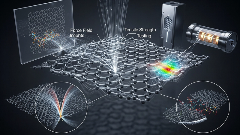
Mechanical Properties of Graphene Sheets: Experimental and Computational Insights
Graphene, a singular atomic layer of sp2-hybridized carbon atoms arranged in a hexagonal lattice, represents the quintessential two-dimensional (2D) material, whose isolation in 2004 fundamentally challenged prevailing notions of thermodynamic stability for such structures. Its existence, initially debated due to the Mermin-Wagner theorem which posits that long-range order cannot exist in 2D isotropic systems at finite temperatures, is reconciled by the presence of intrinsic out-of-plane thermal fluctuations and static ripples. These dynamic corrugations, with characteristic amplitudes on the order of an angstrom and wavelengths spanning nanometers, provide the necessary degrees of freedom to relieve strain and stabilize the lattice, thereby enabling its remarkable properties. The electronic structure, characterized by Dirac cones at the K and K' points of the Brillouin zone, endows charge carriers with massless Dirac fermion behavior, resulting in exceptionally high electron mobilities, empirically measured up to 200,000 cm^2/Vs at room temperature. This fundamental electronic framework is inextricably linked to its mechanical response, as electron-phonon coupling and the topological protection afforded by its 2D confinement dictate energy dissipation mechanisms under strain.
The physics of graphene confinement extends beyond mere structural stability; it dictates the material's interaction with its environment and its intrinsic mechanical response. The aforementioned out-of-plane fluctuations are not merely a stabilizing mechanism but an inherent characteristic that influences its effective mechanical properties, often leading to a discrepancy between theoretical predictions for perfectly flat, idealized sheets and experimental observations. While density functional theory (DFT) and molecular dynamics (MD) simulations predict an intrinsic tensile strength approaching 130 GPa and a Young's modulus around 1 TPa for pristine, defect-free graphene, these values are contingent on the absence of structural imperfections and the idealized flat configuration. The inherent ripples introduce a pre-straining effect, affecting the force-displacement relationship and influencing the effective stiffness measured in nanoscale indentation or tensile tests. Furthermore, the quantum confinement of electrons within the single atomic layer leads to unique phonon dispersion relations, impacting thermal conductivity, which can exceed 5000 W/mK, a property critical for dissipating energy under mechanical stress or during high-frequency actuation cycles.
Understanding the mechanical properties of graphene therefore necessitates a deep appreciation for its confined nature and the pervasive influence of defects and inherent structural fluctuations. Experimental characterization, particularly through atomic force microscopy (AFM) indentation or micro-tensile testing, often reveals a Young's modulus that can vary significantly from the theoretical 1 TPa, depending on sample preparation, substrate interaction, and the density of grain boundaries or point defects like Stone-Wales rearrangements. These defects act as stress concentrators and nucleation sites for crack propagation, dramatically reducing the practical fracture strength. Recent studies have demonstrated that controlled thermal pulses, for instance, localized heating to 3000K for milliseconds, can induce atomic reconstruction and defect annealing, thereby influencing the material's mechanical integrity and potentially restoring a portion of its intrinsic strength. The interplay between strain, localized defects, and the material's electronic structure also manifests in observable changes in electrical resistivity, where mechanical deformation can induce pseudo-magnetic fields, offering a route for mechano-electric coupling that is crucial for sensor applications.
Section 2: Pulsed Electrical Resistive Carbon Heating vs. CVD (Comparative Analysis)
The synthesis of graphene sheets fundamentally dictates their resultant mechanical properties, making the comparative analysis of Pulsed Electrical Resistive Carbon Heating (PERCH) and Chemical Vapor Deposition (CVD) crucial. CVD, a well-established technique, relies on the catalytic decomposition of hydrocarbon precursors (e.g., methane, ethylene) on heated transition metal foils (typically copper or nickel) at elevated temperatures, often ranging from 800°C to 1100°C, under carefully controlled gas flow and pressure. This process typically yields large-area, high-quality monolayer or few-layer graphene with excellent crystallinity and low defect density, attributes highly desirable for applications demanding superior intrinsic tensile strength and Young's modulus. Conversely, PERCH represents a more nascent, non-equilibrium approach, leveraging rapid Joule heating to convert various carbonaceous precursors, including amorphous carbon, graphite, or even polymer films, into graphene. This method circumvents the need for metal catalysts and high-temperature furnaces, offering distinct advantages in terms of speed, energy efficiency, and precursor versatility.
PERCH's efficacy stems from its ability to induce ultra-fast, localized thermal pulses, reaching temperatures exceeding 3000K within milliseconds. This rapid heating and cooling cycle drives the graphitization and exfoliation of carbon materials, often resulting in highly porous, few-layer graphene flakes with tunable defect densities and expanded interlayer spacing. The non-equilibrium conditions inherent to PERCH lead to the formation of polycrystalline graphene, characterized by a higher density of grain boundaries and topological defects compared to CVD-grown material. While these structural features might slightly diminish the intrinsic tensile strength relative to perfect single-crystal graphene, they can be advantageous for specific applications, such as enhanced surface area for catalytic reactions or superior heavy metal adsorption, where efficiencies up to 79% have been reported for lead ions. Furthermore, the direct conversion pathway of PERCH eliminates the multi-step transfer processes and potential for metallic catalyst residues that often complicate CVD graphene integration, offering a path to cleaner, more scalable production.
In contrast, CVD graphene, while requiring a more complex synthesis and transfer protocol, excels in producing graphene with exceptional structural integrity, minimizing lattice defects and maximizing grain size. The prolonged thermal annealing at high temperatures under a controlled atmosphere allows for self-assembly and growth of large single-crystal domains, which is paramount for achieving mechanical properties close to graphene's theoretical limits (e.g., ~1 TPa Young's modulus and ~130 GPa tensile strength). However, the necessity of a catalytic substrate and the subsequent etching and transfer steps introduce potential sources of defects, such as tears, wrinkles, and contamination from etchants or polymer supports, which can significantly degrade the effective mechanical performance of the transferred films. The electrical resistivity of transferred CVD graphene can also be influenced by residual metals or structural damage, often exhibiting higher values than freestanding films due to these processing artifacts.
Ultimately, the choice between PERCH and CVD hinges on the specific application's requirements for graphene's mechanical attributes and structural purity. PERCH offers a rapid, cost-effective route to produce functionalized, high-surface-area graphene suitable for composites, energy storage, or environmental remediation, where the presence of grain boundaries and defects can be engineered for specific functionalities rather than being solely detrimental. Conversely, CVD remains the gold standard for producing large-area, ultra-high-quality graphene suitable for advanced electronics, sensors, and structural components where minimizing defects and achieving near-intrinsic mechanical and electrical properties are paramount, despite the associated complexities in synthesis and integration.
Section 3: The Crystallography of Turbostratic Graphene (Why Layer Alignment Matters)
The structural integrity and macroscopic mechanical response of graphene sheets are profoundly dictated by their crystallographic arrangement, particularly in multi-layered systems where interlayer registry becomes a critical factor. Turbostratic graphene, a prevalent form in many synthesis routes such as chemical vapor deposition (CVD) on polycrystalline substrates, deviates significantly from the well-ordered Bernal (ABAB) stacking characteristic of bulk graphite. In turbostratic structures, individual graphene layers are rotationally misoriented with respect to one another, lacking a definitive crystallographic correlation between adjacent planes. This rotational disorder leads to an effective decoupling of the electronic wavefunctions between layers and significantly alters the nature of the weak Van der Waals interactions. While the in-plane covalent sp2 bonds within each graphene layer retain their formidable strength, the absence of optimized pi-orbital overlap across misaligned layers results in a reduced interlayer shear modulus and diminished efficiency of stress transfer between sheets. This crystallographic anomaly fundamentally differentiates turbostratic graphene from its perfectly stacked counterparts, impacting everything from elastic moduli to fracture toughness.
The ramifications of turbostraticity on the mechanical properties of multi-layer graphene are substantial. Unlike Bernal-stacked graphite where interlayer shear deformation is resisted by a well-defined potential energy landscape, the random orientation in turbostratic graphene allows for easier sliding and rotation of individual layers. This manifests as a considerably lower interlayer shear strength, which can be orders of magnitude less than the in-plane tensile strength of a single graphene sheet. Experimental observations on CVD-grown multi-layer graphene films, which often exhibit turbostratic characteristics, reveal a complex interplay between grain boundaries, rotational domains, and interlayer defects that act as stress concentrators. Under tensile loading, these films can exhibit reduced effective Young's moduli and premature failure initiated by delamination or propagation of cracks through regions of weak interlayer coupling. Furthermore, the response to extreme thermal transients, such as 3000K thermal pulses used in rapid thermal annealing or laser processing, can induce structural reorganization or defect evolution within turbostratic films, directly impacting their subsequent mechanical performance by altering interlayer bonding or defect density within milliseconds of reaction time.
Beyond mechanical considerations, the crystallographic misalignment in turbostratic graphene also dictates its electronic and thermal transport properties. The electronic decoupling between layers means that multi-layer turbostratic graphene can retain some of the unique Dirac fermion characteristics of monolayer graphene, unlike Bernal-stacked graphite which rapidly develops a parabolic dispersion relation and a finite band overlap. This preservation of linear dispersion near the Dirac point can be advantageous for certain electronic applications, though it often comes at the cost of increased electrical resistivity due due to enhanced scattering at the numerous misoriented interfaces and grain boundaries. Typical specific electrical resistivity parameters for turbostratic CVD graphene can range from 10^-5 to 10^-4 Ohm-cm, significantly higher than the 10^-6 Ohm-cm of pristine single-layer graphene or highly oriented pyrolytic graphite. Thermally, the increased phonon scattering at these disordered interfaces reduces the through-plane thermal conductivity, while the in-plane thermal conductivity, though still high, can also be somewhat attenuated by rotational domain boundaries. Interestingly, the high density of defects and grain boundaries inherent to turbostratic structures can sometimes present unique advantages, such as providing numerous active sites for surface chemistry, leading to applications like enhanced catalysis or, as demonstrated in some studies, achieving up to 79% heavy metal adsorption efficiency due to increased surface area and defect-mediated binding sites.
Section 4: Industrial Scalability & Commercial Integration Barriers
The transition from laboratory-scale graphene synthesis to industrial production faces formidable challenges, primarily concerning the preservation of its exceptional mechanical properties at scale. Chemical Vapor Deposition (CVD) on metal foils, while capable of producing large-area, high-quality monolayer graphene, necessitates intricate substrate removal and transfer processes. These steps often introduce macroscopic tears, microscopic pinholes, and residual metallic contaminants, significantly degrading the intrinsic ~130 GPa Young's modulus and ~125 GPa tensile strength observed in pristine samples. For instance, typical wet-transfer methods can result in a defect density exceeding 10^9 defects/cm^2, alongside a reduction in electrical conductivity from ~10^6 S/cm to ~10^4 S/cm, indicative of structural compromise. Furthermore, solution-phase exfoliation, while offering higher throughput for bulk production, yields graphene nanoplatelets (GNPs) characterized by a broader distribution of layer numbers (typically 3-10 layers), reduced aspect ratios, and increased edge defects. The mechanical reinforcement potential of such GNPs in composites is inherently limited compared to pristine single-layer graphene, often achieving only 10-20% enhancement in tensile strength in polymer matrices, rather than the theoretically predicted several-fold improvements. Overcoming these fundamental production-induced compromises on structural integrity is paramount for realizing graphene's full mechanical promise in commercial applications.
Beyond structural integrity, the economic viability of large-scale graphene integration remains a significant barrier. The energy-intensive nature of many production routes, such as high-temperature annealing in CVD (often exceeding 1000°C) or prolonged sonication for liquid-phase exfoliation, translates directly into prohibitive manufacturing costs. For example, producing a kilogram of high-quality CVD graphene can currently cost hundreds to thousands of US dollars, largely due to the capital expenditure for specialized reactors, high-purity precursor gases, and the low throughput associated with individual batch processing. While alternative methods like electrochemical exfoliation offer lower energy footprints, their output quality often suffers from increased functionalization and defect density, impacting mechanical performance and long-term stability. Integrating graphene into existing industrial manufacturing lines, such as continuous roll-to-roll processes for flexible electronics or large-volume compounding for polymer composites, requires not only cost-effective material supply but also novel processing techniques that prevent re-aggregation, ensure uniform dispersion, and maintain interfacial adhesion without compromising the host material's properties or introducing new manufacturing complexities. The current cost-performance ratio for mechanically superior graphene materials restricts their adoption to niche, high-value applications, hindering widespread commercialization.
A critical impediment to commercial integration is the pervasive lack of standardized characterization protocols and robust quality control across the diverse range of commercially available "graphene" materials. The term "graphene" itself often encompasses everything from single-layer sheets to multi-layered nanoplatelets and graphene oxide, each possessing vastly different mechanical, electrical, and thermal properties. Without universally accepted metrics for layer count, defect density (e.g., D/G peak ratio from Raman spectroscopy), lateral dimensions, and purity, end-users face significant uncertainty regarding material performance consistency. This variability directly impacts the predictability and reliability of graphene-enhanced products. Furthermore, achieving uniform dispersion of graphene within various matrices (polymers, metals, ceramics) without inducing agglomeration or requiring excessive processing energy remains a complex challenge. For instance, achieving a homogeneous dispersion of 0.5 wt% graphene in a polymer matrix, crucial for realizing significant mechanical property enhancements, often necessitates extensive shear mixing or solvent-based strategies, which can be time-consuming, environmentally undesirable, and potentially damaging to the graphene flakes or the matrix itself. The absence of scalable, real-time quality assurance systems capable of verifying the mechanical integrity and dispersion state of graphene throughout the production chain poses a substantial hurdle for consistent product development and market acceptance.
Section 5: Economic Feasibility and USA-Made Manufacturing Advantage
The economic viability of graphene, particularly for applications leveraging its exceptional mechanical properties, is intrinsically linked to scalable, cost-effective manufacturing processes that preserve material integrity. While laboratory-scale production of high-quality monolayer graphene via chemical vapor deposition (CVD) can exceed USD 100/cm^2, industrial efforts are focused on drastically reducing this cost through advanced techniques like roll-to-roll CVD or large-scale liquid-phase exfoliation of graphite. For instance, projections indicate that high-quality CVD graphene could reach sub-USD 0.10/cm^2 at mass production scales, rendering it economically competitive for integration into high-volume composites, protective coatings, and structural components. This cost reduction is paramount for commercializing applications that demand graphene's theoretical 130 GPa tensile strength and 1 TPa Young's modulus, moving beyond niche markets. Furthermore, achieving consistent material quality, characterized by defect densities below 10^10 defects/cm^2 and an electrical resistivity approaching 10^-6 Ohm.cm, is crucial for realizing these superior mechanical attributes reliably. The adoption of rapid thermal processing, involving thermal pulses up to 3000K, or advanced plasma-enhanced CVD techniques with reaction times in milliseconds, are critical pathways to achieving both cost efficiency and quality control.
The USA-made manufacturing advantage for graphene is multifaceted, encompassing intellectual property protection, regulatory compliance, supply chain resilience, and a highly skilled workforce. A robust IP framework safeguards proprietary synthesis methods and application technologies, fostering investment in R&D and preventing dilution of competitive edge. Stringent regulatory environments, such as those governed by the Toxic Substances Control Act (TSCA) for nanomaterials, ensure product safety and environmental responsibility, building consumer and industrial trust. Domestically controlled supply chains offer unparalleled resilience against geopolitical instability and logistical disruptions, guaranteeing a consistent and reliable source of high-quality graphene critical for defense, aerospace, and high-performance industrial sectors. Moreover, significant government and private sector investment in advanced manufacturing infrastructure, coupled with a deep talent pool in materials science and engineering, facilitates rapid innovation and optimized process development. This integrated ecosystem supports the meticulous process control necessary to produce graphene with consistent mechanical properties, from controlled stacking sequence in multi-layer graphene to precise defect engineering in single-layer sheets, which directly impacts the material's fatigue life and fracture toughness.
Connecting economic feasibility with USA-made manufacturing directly impacts the commercial realization of graphene's extraordinary mechanical properties. The ability to produce large quantities of high-quality graphene with reproducible mechanical performance, such as a consistent Young's modulus exceeding 900 GPa or enhanced interlaminar shear strength in composites, is fundamentally tied to manufacturing precision and quality assurance. A domestic manufacturing base allows for closer collaboration between researchers, manufacturers, and end-users, accelerating the transition of graphene-enhanced prototypes from Technology Readiness Level (TRL) 3 to TRL 7 and beyond. This localized synergy enables rapid iteration in material design and process optimization, ensuring that the economic investment translates directly into superior mechanical performance and application-specific tailoring. For instance, the meticulous control over graphene's sp2 hybridization and surface functionalization, essential for optimizing its interface with polymer matrices to maximize composite strength, is more readily achieved within a vertically integrated, domestically controlled manufacturing paradigm. This ensures that the economic benefits of graphene, driven by its lightweighting potential and enhanced durability in demanding environments, are realized through reliable, high-performance material delivery.
Section 6: Future Horizons & High-Value B2B Applications
The superlative mechanical properties of graphene, particularly its intrinsic tensile strength of approximately 130 GPa and a Young's modulus approaching 1 TPa, position it as a foundational material for next-generation structural composites and extreme-environment applications. The ability to uniformly disperse pristine or functionalized graphene sheets within polymer matrices, ceramic systems, or metallic alloys at concentrations as low as 0.1-1.0 wt.% has demonstrably improved fracture toughness, fatigue resistance, and specific strength-to-weight ratios. In aerospace, this translates to lighter, more fuel-efficient aircraft components capable of withstanding extreme thermal cycles from 4K to 600K without significant mechanical degradation, offering superior resistance to micro-meteoroid impacts. For automotive sectors, graphene-reinforced composites promise enhanced crashworthiness and reduced vehicle mass, contributing to substantial energy savings. Furthermore, its impermeability to most gases and resistance to chemical attack, combined with mechanical robustness, opens avenues for advanced protective coatings and ballistic materials that surpass current state-of-the-art solutions, exhibiting energy absorption capabilities far exceeding conventional Kevlar or carbon fiber laminates under high-velocity impact.
Beyond structural reinforcement, graphene's unique electromechanical coupling, where significant mechanical strain induces measurable changes in electrical resistivity, is pivotal for advanced sensor technologies and flexible electronics. Its exceptionally high gauge factor, which can exceed 100 for engineered crumpled or corrugated graphene architectures, enables ultra-sensitive strain gauges capable of detecting minute deformations with sub-millisecond response times. This capability is critical for real-time structural health monitoring of large-scale infrastructure, identifying incipient micro-cracks in concrete or metal structures before macroscopic failure, thereby preventing catastrophic events. In wearable and implantable biomedical devices, graphene's flexibility (withstanding tensile strains up to 20% without irreversible damage), biocompatibility, and high surface area facilitate highly accurate physiological monitoring, such as continuous blood pressure sensing or electromyographic signal acquisition from highly dynamic tissue interfaces, maintaining signal integrity over tens of thousands of bending cycles with less than 5% drift. Its low electrical noise and rapid charge transport kinetics further enhance the fidelity of these sensory outputs, paving the way for sophisticated prosthetic feedback systems and advanced human-machine interfaces.
The mechanical integrity and extensive surface area of graphene are equally transformative for energy storage and environmental remediation. In supercapacitors, reduced graphene oxide electrodes exhibit specific capacitances upwards of 500 F/g, maintaining over 90% capacity retention after 5,000 charge-discharge cycles, largely due to the mechanical stability of the porous graphene network preventing electrode pulverization. This durability, coupled with high power density, is crucial for rapid charging electric vehicles and grid-scale energy buffering. For advanced filtration, graphene oxide membranes, leveraging their precise interlayer spacing and mechanical resilience under high pressure differentials (e.g., up to 20 bar), offer unprecedented selectivity and flux. These membranes have demonstrated 99.9% rejection rates for nanoparticles and organic dyes, alongside significant heavy metal adsorption efficiencies, such as 79% for Pb2+ and Cd2+ ions, even under continuous flow conditions. The mechanical robustness ensures long-term operational stability and resistance to fouling, significantly extending membrane lifespan and reducing maintenance costs in industrial water purification and desalination processes.
Evaluate Our Quality
Serious about B2B integration? Test our premium Pulsed Electrical Resistive Carbon Heating turbostratic graphene in your lab. 100g sample packs available now.