Mastering Graphene Device Fabrication: Precision Processing for 2D Materials
Mastering Graphene Device Fabrication: Precision Processing for 2D Materials
The advent of graphene, a groundbreaking two-dimensional material, has ignited a revolution across numerous scientific and engineering disciplines. Its extraordinary properties—unrivaled electron mobility, exceptional strength, and transparent conductivity—position it as a cornerstone for next-generation electronic, optical, and mechanical devices. However, translating these theoretical advantages into practical, high-performance applications hinges critically on the ability to precisely manipulate and integrate this atomically thin material. This is where the intricate science of graphene device fabrication comes into play, demanding a meticulous approach that acknowledges graphene’s unique nanoscale characteristics.
While the foundational principles of semiconductor fabrication provide a valuable starting point, the processing of graphene introduces a distinct set of challenges and considerations. Unlike bulk silicon, graphene’s single-atom thickness makes it extraordinarily sensitive to its environment and processing conditions. From the initial choice of production method and substrate to the delicate steps of patterning, resist application, and metal contact formation, each stage requires careful adaptation and optimization to preserve graphene’s inherent superlative properties. Understanding these nuanced fabrication considerations is paramount for researchers and engineers aiming to unlock the full potential of graphene in real-world applications.
This comprehensive guide delves into the essential design rules and process integration strategies for graphene devices, drawing from established research in the field. We will explore the critical decisions involved in material production, the high-precision lithographic techniques required for nanoscale patterning, the often-overlooked but crucial aspects of resist management, and the complexities of forming robust, low-resistance metal contacts. By dissecting these core elements, we aim to provide a clear roadmap for navigating the intricacies of graphene processing, empowering innovators to push the boundaries of 2D material technology.
Strategic Graphene Production: Choosing the Right Foundation
The journey of graphene device fabrication begins with the selection of an appropriate graphene production technique, a decision heavily influenced by the desired application and the critical balance between material quality and scalability. Various methods exist, each offering distinct advantages and trade-offs. For instance, mechanical exfoliation from graphite, the pioneering method, yields graphene with the highest carrier mobilities, often exceeding 200,000 cm2 V−1 s−1 in ideal conditions. This makes exfoliated graphene ideal for fundamental research and high-performance laboratory prototypes where ultimate material quality is paramount, despite its inherent limitation in terms of scalability for mass production.
In contrast, chemical vapor deposition (CVD) on transition metals like copper or nickel offers a highly scalable route for producing large-area graphene films. While CVD graphene typically requires a subsequent transfer process to an insulating substrate, it represents a viable pathway for industrial applications demanding wafer-scale production. Another significant method is epitaxial growth on silicon carbide (SiC), which can produce high-quality graphene directly on an insulating or semi-insulating substrate. This eliminates the need for a transfer step, simplifying the device fabrication process. However, a key consideration for epitaxial graphene is the potential for substrate interaction between the graphene layer and the SiC, which can subtly affect the electronic structure and carrier transport properties of the graphene.
The choice of the underlying substrate is equally critical and profoundly impacts device performance. While silicon dioxide (SiO2) on silicon wafers is a common and readily available substrate for transferred graphene flakes or CVD films, it presents inherent challenges. SiO2 surfaces often exhibit charge traps and surface roughness, which can limit the practically obtainable electron mobility in graphene devices to around 15,000 cm2 V−1 s−1. This is a significant reduction compared to graphene’s theoretical mobility. To mitigate these issues, alternative substrates such as hexagonal boron nitride (h-BN) are increasingly employed. h-BN offers an atomically flat surface with minimal charge traps, providing a cleaner electrical environment that helps preserve graphene’s intrinsic high mobility and reduces scattering effects, thereby enhancing device performance.
Ultimately, the selection of a graphene production method and substrate must align with the specific requirements of the intended device. For high-frequency electronics or sensitive sensors, the superior quality of exfoliated or h-BN-supported graphene might be indispensable, even if it means sacrificing scalability. For transparent electrodes or flexible electronics, the cost-effectiveness and large-area capabilities of CVD graphene might take precedence. A thorough understanding of these foundational choices is the first step toward successful graphene device fabrication.
High-Precision Patterning: Lithographic Techniques for Graphene
Patterning graphene with high precision is an indispensable step in graphene device fabrication, allowing the creation of intricate device architectures from simple transistors to complex integrated circuits. The atomically thin nature of graphene necessitates the use of advanced lithographic techniques, primarily electron beam lithography (EBL) and photolithography, adapted from conventional semiconductor processing. Each method offers distinct capabilities and trade-offs regarding resolution, throughput, and cost, dictating their suitability for different stages of research and development.
Electron beam lithography (EBL) stands out for its unparalleled resolution, capable of defining features as small as approximately 10 nanometers. This makes EBL the preferred technique for fabricating nanoscale graphene devices, such as quantum dots, nanoribbons, or ultra-small transistors, where quantum effects and precise geometry are critical. EBL offers exceptional versatility, allowing for direct writing of custom patterns without the need for a physical mask, which is ideal for rapid prototyping and academic research. However, its primary drawback is its inherently low throughput, as patterns are drawn serially point-by-point. This makes EBL economically unfeasible for large-scale production, confining its use predominantly to research and development environments where high resolution outweighs speed.
In contrast, photolithography is the workhorse of industrial semiconductor manufacturing, renowned for its high throughput and ability to pattern entire wafers simultaneously. This technique utilizes ultraviolet light projected through a photomask to transfer patterns onto a resist-coated substrate. While photolithography offers significantly higher throughput and lower cost per device compared to EBL, its resolution is limited by the wavelength of light used, typically yielding feature sizes greater than those achievable with EBL. For graphene, photolithography is often employed for patterning larger features, defining contact pads, or creating arrays of devices where the highest nanoscale resolution is not strictly required. The integration of photolithography into graphene device fabrication is crucial for scaling up production and reducing manufacturing costs, bridging the gap between research prototypes and commercial viability.
Both EBL and photolithography rely on resists, which are light- or electron-sensitive polymers that protect specific areas of graphene during subsequent etching or deposition steps. The careful selection and application of these resists are paramount, as the interaction between the resist and the single-atom-thick graphene layer can have profound consequences. Unlike bulk materials, graphene is highly susceptible to contamination and damage from resist processing. Therefore, meticulous attention must be paid to ensure complete and clean removal of resist residues, as even minute amounts can severely degrade device performance, a critical challenge we will explore in further detail.
The Invisible Barrier: Conquering Resist Residue and Etching Challenges
One of the most persistent and often underestimated challenges in graphene device fabrication is the complete removal of polymer resist layers after lithographic patterning. While standard lithographic methods are routinely applied, the unique two-dimensional nature of graphene makes it exquisitely sensitive to processing residues. Even minute, seemingly invisible amounts of resist residue can act as charge traps, scattering centers, or unwanted doping agents, significantly compromising the electrical, optical, and mechanical performance of the final graphene device. This necessitates a departure from conventional resist removal protocols, demanding specialized techniques and rigorous validation.
Residues can adhere strongly to the graphene surface, especially after exposure to high-energy electron beams in EBL or intense UV light in photolithography, which can cross-link the polymer chains and make them harder to dissolve. These persistent polymer fragments can create an unwanted dielectric layer, altering the local electrostatic environment and hindering charge transport. They can also impede the formation of clean, low-resistance metal contacts by creating an insulating barrier between the metal and the graphene, leading to increased contact resistance (RC) and non-Ohmic behavior. Furthermore, residues can introduce uncontrolled doping, shifting the Dirac point and making device characteristics unpredictable. Therefore, achieving pristine graphene surfaces post-lithography is a non-negotiable requirement for high-performance devices.
Effective resist removal strategies often involve a combination of solvent-based cleaning and gentle physical or chemical treatments. Traditional solvent baths (e.g., acetone, NMP) may not be sufficient to remove all residues, especially those that are partially cross-linked. Advanced techniques include plasma cleaning (e.g., low-power oxygen plasma), thermal annealing in inert atmospheres, or even critical point drying. However, each method must be carefully optimized to avoid damaging the delicate graphene lattice itself. Excessive plasma exposure can etch graphene, while high-temperature annealing might cause unwanted chemical reactions or delamination. The goal is a process that effectively removes all organic contaminants without introducing defects or altering the intrinsic properties of the graphene. This often requires iterative experimentation and characterization using techniques like atomic force microscopy (AFM) or Raman spectroscopy to confirm surface cleanliness.
Beyond resist removal, etching is another critical step in patterning graphene, typically employed to define the physical boundaries of the device. Both dry etching (e.g., reactive ion etching with oxygen plasma) and wet etching can be used. Dry etching offers anisotropic control and higher resolution, but careful control of plasma power and etch time is essential to prevent over-etching or plasma-induced damage to the remaining graphene. A significant concern in etching at the nanoscale is Line Edge Roughness (LER). LER refers to the jaggedness of the etched edges of the graphene feature. High LER can degrade device performance by introducing additional scattering sites, increasing electrical resistance, and altering the effective width of nanodevices. Minimizing LER requires precise control over the resist profile, etch chemistry, and process parameters, highlighting the intricate interplay of various fabrication steps in achieving optimal graphene device performance.
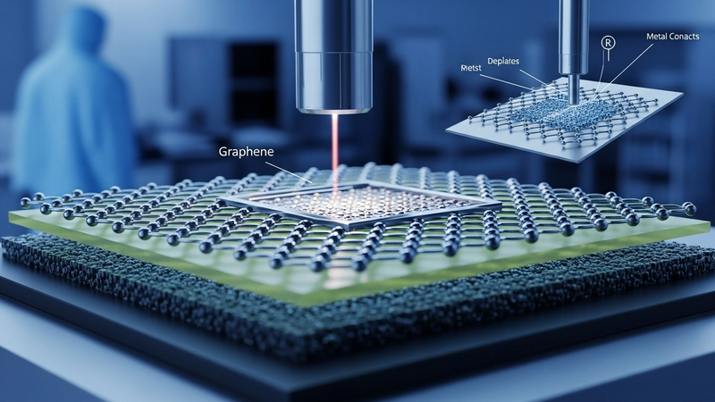
Forging the Connection: Optimizing Metal Contacts for Graphene Devices
The formation of reliable, low-resistance metal contacts is a cornerstone of any electronic device, and in graphene device fabrication, this aspect presents particularly complex challenges. Unlike conventional semiconductors where Ohmic contacts are relatively straightforward to achieve, the two-dimensional nature and unique electronic band structure of graphene make the formation of an ideal Ohmic contact a non-trivial task. An Ohmic contact is characterized by a linear current-voltage (I-V) relationship and minimal resistance at the metal-semiconductor interface, ensuring efficient charge injection and extraction without introducing significant voltage drops or non-linearities that degrade device performance.
One of the primary difficulties stems from the inherent contact resistance (RC) at the metal-graphene interface. Even if the metal-graphene interface itself is perfectly Ohmic, the resistance of the contact region can still be substantial due to factors such as the work function mismatch between the metal and graphene, the presence of surface contaminants (including residual resist), and the doping effect of the metal. A high RC can dominate the total device resistance, especially in short-channel devices, negating the advantages of graphene’s high intrinsic mobility. Therefore, meticulous engineering of the metal-graphene interface is crucial to minimize RC and ensure efficient device operation, directly impacting the overall speed and power consumption of graphene-based electronics.
Furthermore, graphene is highly susceptible to contact doping by adjacent metal contacts. The work function difference between the metal and graphene can induce a charge transfer, effectively doping the graphene locally. Different metals can effect either p-type or n-type doping in graphene, depending on whether their work function is higher or lower than graphene’s Dirac point. For instance, metals with higher work functions (e.g., palladium, platinum) tend to p-dope graphene, while those with lower work functions (e.g., titanium, aluminum) can n-dope it. This localized doping can create unwanted p-n junctions at the contact interface, leading to Schottky barriers that impede current flow and introduce rectifying behavior, further increasing RC. Understanding and controlling this doping effect is vital for designing functional graphene devices with predictable electrical characteristics.
Strategies to improve contact resistance and mitigate doping effects include careful selection of contact metals, interface engineering, and post-deposition treatments. Metals like palladium (Pd) or titanium (Ti) with a thin overlay of gold (Au) are commonly used, chosen for their adhesive properties and relatively favorable work functions. Interface engineering, such as inserting ultra-thin dielectric layers or pre-treating the graphene surface, can help reduce charge transfer and improve contact quality. Post-deposition annealing in an inert atmosphere is also frequently employed to improve adhesion, reduce interface defects, and sometimes even modify the work function of the metal, leading to lower RC. Techniques like the Transfer Length Method (TLM) are routinely used to experimentally measure and quantify contact resistance, providing critical feedback for optimizing the metal contact fabrication process and ensuring the integrity of the overall graphene device fabrication flow.
Adapting Semiconductor Paradigms: Key Considerations for Graphene Device Integration
The overarching theme in graphene device fabrication is the intelligent adaptation of mature semiconductor processing techniques to the unique demands of a 2D material. While silicon-based CMOS fabrication flows provide a robust framework, direct application without modification often leads to suboptimal or non-functional graphene devices. The fundamental difference lies in the material’s dimensionality: silicon is a bulk material, whereas graphene is a surface-dominated material, making it highly sensitive to every processing step, from substrate interaction to resist chemistry and metallization.
A critical consideration throughout the process flow is the substrate selection and its interaction with graphene. As previously discussed, the choice between conventional SiO2 and advanced materials like h-BN directly impacts carrier mobility and device stability. Beyond the intrinsic material properties, even the gate dielectric, often a thin insulating layer, plays a crucial role. Its quality, interface traps, and dielectric constant directly influence the electrostatic gating efficiency and overall performance of graphene field-effect transistors. Therefore, the integration of the gate dielectric must be carefully designed to minimize defects and maximize gate coupling, a process that might require novel deposition techniques or surface treatments not typically encountered in bulk semiconductor processing.
The entire process flow for graphene devices, while following a sequence familiar to semiconductor engineers (e.g., cleaning, deposition, lithography, etching, metallization), requires constant vigilance regarding potential damage mechanisms. For instance, aggressive plasma etching or high-temperature annealing steps, routine in silicon processing, can easily introduce defects, vacancies, or edge damage in graphene, significantly degrading its performance. The design rules for graphene devices must therefore incorporate lower thermal budgets, gentler chemical treatments, and precise control over plasma parameters to preserve the material's integrity. This iterative process of adapting and refining each step is central to successful graphene device fabrication.
Moreover, the scalability of the chosen fabrication methods is a significant factor, especially when moving beyond laboratory prototypes. While techniques like EBL are essential for exploring fundamental physics at the nanoscale, their low throughput makes them unsuitable for industrial production. Integrating high-throughput methods like photolithography or even alternative lithography-free techniques (e.g., direct laser writing, inkjet printing for certain applications) becomes crucial for commercial viability. This requires a holistic view of the entire fabrication chain, ensuring that each step is not only technically feasible for graphene but also economically scalable. The continuous evolution of graphene device fabrication is a testament to the ongoing efforts to harmonize the unparalleled properties of 2D materials with the rigorous demands of industrial-scale semiconductor manufacturing, paving the way for a new era of advanced electronics and beyond.
FAQ: Graphene Device Fabrication Insights
Q1: Why is resist removal so critical for graphene devices compared to traditional semiconductors?
Resist removal is exceptionally critical for graphene because its single-atom thickness makes it highly susceptible to contamination. Even minute residues can act as charge traps, scatter electrons, or create an insulating barrier, significantly degrading the electrical performance, increasing contact resistance, and introducing unpredictable doping effects in the ultra-sensitive 2D material.
Q2: What are the main trade-offs in different graphene production methods?
The primary trade-offs involve material quality versus scalability. Mechanical exfoliation yields the highest quality graphene (e.g., >200,000 cm2 V−1 s−1 mobility) but is not scalable. Chemical Vapor Deposition (CVD) is scalable for large areas but requires a transfer step and may have lower initial quality. Epitaxial growth on SiC offers high quality on an insulating substrate but can suffer from substrate interaction effects.
Q3: How do metal contacts affect graphene's electronic properties?
Metal contacts significantly impact graphene's electronic properties primarily through contact resistance (RC) and contact doping. RC impedes efficient charge transfer, while the work function difference between the metal and graphene can induce localized p- or n-type doping, creating unwanted Schottky barriers and altering the intrinsic electronic characteristics of the device.
Q4: What are the advantages and disadvantages of Electron Beam Lithography (EBL) versus Photolithography for graphene patterning?
EBL offers superior resolution (down to 10 nm) and maskless patterning, ideal for nanoscale research and prototyping, but suffers from very low throughput. Photolithography provides high throughput for wafer-scale patterning, making it suitable for industrial applications, but is limited to larger feature sizes than EBL and requires a photomask.
Q5: Why are standard semiconductor processing techniques not directly applicable to graphene?
Standard semiconductor techniques, designed for bulk materials, require adaptation for graphene due to its 2D nature. Graphene's atomic thickness makes it extremely sensitive to process-induced damage (e.g., from harsh plasmas or high temperatures), contamination from resist residues, and strong interaction with the underlying substrate, all of which necessitate gentler, more precise fabrication protocols.
Unlock the Future of Graphene with usa-graphene.com
The journey through graphene device fabrication reveals a landscape rich with both immense potential and intricate challenges. From the meticulous selection of production methods and substrates to the precision required in lithographic patterning, the careful management of resist residues, and the sophisticated engineering of metal contacts, each step is critical in harnessing the extraordinary properties of this 2D material. Successful integration demands a deep understanding of graphene’s unique physics and a willingness to adapt established semiconductor paradigms to its nanoscale realities. The future of advanced electronics, sensors, and quantum technologies hinges on our ability to master these fabrication complexities.
At usa-graphene.com, we are at the forefront of this technological frontier, providing high-quality graphene materials and expert insights to power your innovations. Whether you are a researcher pushing the boundaries of fundamental science or an engineer developing next-generation devices, understanding the nuances of graphene device fabrication is paramount. Partner with us to ensure your projects benefit from the highest quality graphene and the most advanced processing knowledge. Explore our offerings and let us help you transform the promise of graphene into tangible, high-performance solutions. Visit usa-graphene.com today to learn more and connect with our team of experts.
Evaluate Our Quality
Serious about B2B integration? Test our premium Pulsed Electrical Resistive Carbon Heating turbostratic graphene in your lab. 100g sample packs available now.