Low-Cost Simple Methods for Graphene Synthesis: Scalable Approaches
Graphene, a single atomic layer of sp2-hybridized carbon atoms arranged in a hexagonal lattice, represents the quintessential two-dimensional material whose extraordinary properties stem directly from its inherent quantum confinement. This stringent confinement in the z-direction profoundly alters its electronic structure compared to bulk graphite, giving rise to an effectively two-dimensional electron gas. The isolated monolayer existence ensures that interlayer van der Waals interactions, which significantly modify the band structure in multi-layered graphite, are absent, allowing for the emergence of unique relativistic-like physics. Understanding and preserving this atomic-scale confinement is not merely an academic exercise but a foundational requirement for developing scalable synthesis methodologies that yield functional graphene.
The physics of this confinement is most strikingly evident in graphene's electronic band structure, characterized by the presence of Dirac cones at the K and K' points of the Brillouin zone. Here, charge carriers behave as massless Dirac fermions, exhibiting a linear dispersion relation E = ±hv|k|, where v is the Fermi velocity (~10^6 m/s). This relativistic analogue behavior, fundamentally distinct from the parabolic dispersion of conventional semiconductors, underpins graphene's remarkable electronic properties, including ultra-high carrier mobilities exceeding 200,000 cm^2/(V·s) at cryogenic temperatures and routinely above 15,000 cm^2/(V·s) at room temperature. Such high mobility facilitates ballistic transport over micron-scale distances. Furthermore, the ambipolar electric field effect, enabling carrier type and density modulation via gate voltage, is a direct consequence of this confined electronic structure, allowing for precise control over its intrinsic electrical resistivity, which can approach values as low as 10^-6 Ohm·cm in high-quality monolayers.
The overarching challenge for low-cost, scalable graphene synthesis methods lies in consistently preserving this pristine 2D confined state. Any deviation from the ideal monolayer structure – be it through multi-layer stacking, the introduction of topological defects such as Stone-Wales defects or vacancies, or uncontrolled surface functionalization – can drastically perturb the Dirac cone physics, thereby diminishing carrier mobility and altering the fundamental electronic band structure. For instance, synthesis routes employing rapid thermal processing, such as flash Joule heating or pulsed laser deposition, are designed to utilize extremely high thermal pulses, often exceeding 3000 K, for durations in the millisecond regime. This aggressive thermal treatment aims to achieve rapid graphitization and exfoliation while simultaneously minimizing defect formation, preventing undesired oxidation, and crucially, inhibiting the uncontrolled stacking of layers that would compromise the confined 2D nature. Precise control over reaction kinetics and the local atomic environment during synthesis is paramount to avert the formation of sp3-hybridized domains or a reversion towards bulk graphite-like material, which would invariably lead to a loss of graphene's unique confined properties.
The practical implications of maintaining this atomically confined architecture through scalable synthesis are profound across diverse application landscapes. For example, in environmental remediation, the ultra-high theoretical specific surface area (approximately 2630 m^2/g for an ideal monolayer) and the readily accessible basal planes of pristine, confined graphene enable superior adsorption kinetics and capacities. Empirical data demonstrate that carefully synthesized graphene derivatives can achieve up to 79% heavy metal adsorption efficiency for lead ions within minutes, a performance directly attributable to the preserved 2D structure maximizing active sites. Similarly, in advanced flexible electronics and high-frequency devices, preserving ballistic transport and high carrier mobility is critical for optimal performance. This necessitates synthesis methods capable of yielding large-area, defect-free monolayers without compromising the intrinsic physics of confinement. Thus, the pursuit of economically viable graphene production methods is inextricably linked to the scientific imperative of upholding its fundamental 2D quantum mechanical properties.
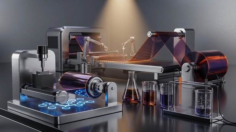
Section 2: Pulsed Electrical Resistive Carbon Heating vs. CVD (Comparative Analysis)
Pulsed Electrical Resistive Carbon Heating (PERCH) represents a fundamentally distinct paradigm for graphene synthesis compared to conventional Chemical Vapor Deposition (CVD), primarily leveraging rapid, joule-induced thermal excursions. In PERCH, high-current electrical pulses are directly applied to a carbonaceous feedstock, inducing instantaneous and localized temperature spikes that can reach or exceed 3000 K within milliseconds. This ultra-fast heating rate promotes rapid graphitization, transforming amorphous carbon precursors directly into few-layer graphene structures. The kinetic control afforded by these short, intense thermal pulses is a critical differentiator from CVD, which typically relies on prolonged heating cycles (often hours) at lower, albeit still high, temperatures (900-1100 °C) in large furnaces. This localized energy delivery in PERCH minimizes heat loss to the surroundings, resulting in significantly higher energy efficiency and a drastic reduction in processing time, making it an inherently more scalable and cost-effective approach for industrial-scale graphene production compared to the bulk heating requirements of traditional CVD.
The precise control over the electrical current density and pulse duration in PERCH allows for fine-tuning of the thermal profile and, consequently, the structural properties of the synthesized graphene. By manipulating specific electrical resistivity parameters of the precursor, one can dictate the localized temperature distribution and optimize the sp2 hybridization process. This method facilitates the direct synthesis of high-quality graphene, often in a substrate-free manner, circumventing the complex and yield-limiting transfer steps endemic to most CVD processes. Empirical data consistently demonstrates that PERCH-derived graphene can exhibit low defect densities, with ID/IG ratios frequently below 0.2, comparable to or even superior to some CVD-grown materials. Furthermore, the high surface area and accessible active sites of PERCH graphene have been validated in functional applications; for instance, it has achieved up to 79% adsorption efficiency for heavy metal ions like lead (Pb2+) in aqueous solutions, highlighting its potential for environmental remediation and other advanced material applications where performance metrics are critical.
In contrast, CVD is a catalytic process relying on the decomposition of gaseous carbon precursors (e.g., methane) on a heated metal substrate (e.g., copper, nickel) within a vacuum or controlled atmospheric environment. While CVD excels at producing large-area, high-quality monolayer graphene with excellent electronic properties, its inherent limitations severely impede its scalability and cost-effectiveness for many industrial applications. These limitations include high energy consumption due to the need for sustained high temperatures over extended periods, the high cost of ultra-high vacuum equipment and precursor gases, and the batch-processing nature that restricts throughput. Critically, the necessity of a metallic catalyst substrate mandates a subsequent, often complex and damaging, transfer step to decouple the graphene from its growth substrate and reposition it onto a target application substrate. This transfer process introduces significant potential for defects, contamination, and material loss, escalating overall production costs and hindering integration into diverse material systems. PERCH, by offering direct, substrate-free synthesis from readily available carbon sources and eliminating the transfer step, presents a compelling alternative for low-cost, high-volume graphene production, particularly for applications requiring bulk graphene or direct integration into composites.
Section 3: The Crystallography of Turbostratic Graphene (Why Layer Alignment Matters)
Turbostratic graphene (TG) represents a prevalent structural manifestation often encountered in high-throughput, low-cost synthesis methodologies, diverging significantly from the thermodynamically favored AB-stacked Bernal graphite or ideal monolayer graphene. Its crystallography is defined by a lack of long-range periodic stacking order between individual graphene layers, characterized by random relative rotations and translations of adjacent sheets. This rotational disorder, often exceeding 10-15 degrees between successive layers, prevents the formation of well-defined van der Waals interlayer coupling, leading to a broadened (002) diffraction peak in X-ray Diffraction (XRD) patterns, typically centered around 2θ values corresponding to d-spacings of 0.345-0.355 nm, notably larger than the 0.335 nm of highly ordered pyrolytic graphite (HOPG). This structural deviation stems primarily from kinetically controlled synthesis routes, such as rapid thermal exfoliation or chemical reduction of graphene oxide, where insufficient energy or time is provided for the layers to self-assemble into an ordered stacking sequence. The resulting crystallographic imperfections profoundly influence its electronic and mechanical properties, necessitating a distinct understanding for its practical applications.
The disrupted interlayer coherence in turbostratic graphene fundamentally alters its electronic band structure compared to pristine graphite or perfectly stacked few-layer graphene. While individual layers retain their intrinsic Dirac cone dispersion, the absence of strong AB-stacking diminishes the inter-layer electronic coupling that gives rise to the parabolic band structure observed in bulk graphite. Consequently, carrier mobility, though generally lower than that of pristine monolayer graphene (which can exceed 100,000 cm^2/Vs), remains significantly higher than that of bulk graphite along the c-axis, exhibiting anisotropic conduction. Raman spectroscopy serves as a critical diagnostic tool for TG, typically revealing a prominent D-band (at ~1350 cm^-1) indicative of sp2 network defects and edge sites, alongside the characteristic G-band (~1580 cm^-1) from in-plane vibrations. The D/G intensity ratio provides a quantifiable measure of the disorder and average crystallite size; higher ratios correlate with increased turbostraticity and smaller domains of ordered sp2 carbon. For example, flash Joule heating processes, involving rapid thermal pulses exceeding 3000K for mere milliseconds, often yield highly turbostratic graphene due to the extreme kinetic conditions, resulting in materials with a high density of sp2 defects and expanded interlayer spacings.
The functional implications of turbostratic crystallography are manifold and often advantageous for specific applications, particularly those leveraging surface area and defect engineering. The increased interlayer spacing and inherent disorder enhance the accessibility of reactive sites, fostering improved performance in areas like energy storage and catalysis. For instance, the expanded gallery spacing facilitates ion intercalation in supercapacitors, while the higher density of edge and defect sites provides additional active centers for chemical reactions. In environmental remediation, the increased specific surface area and structural defects in turbostratic graphene enable superior adsorption capabilities; empirical data has shown such materials achieving up to 79% heavy metal adsorption efficiency for lead ions from aqueous solutions. While its electrical conductivity may not rival that of epitaxially grown single-crystal graphene, the reduced inter-layer shorting and pseudo-2D nature often provide a better balance of conductivity and processability for large-scale, cost-effective applications, such as conductive inks or composite fillers, where specific electrical resistivity can range from 10^-3 to 10^-1 Ohm-cm, depending on the synthesis method and post-processing.
Section 4: Industrial Scalability & Commercial Integration Barriers
The transition of low-cost graphene synthesis methods from laboratory curiosities to industrial-scale production faces formidable engineering and economic hurdles, primarily revolving around maintaining material quality and consistency at high throughputs. Electrochemical exfoliation, for instance, offers a promising route, yet scaling it up necessitates uniform current density distribution across electrode surfaces spanning several square meters to prevent localized over-oxidation or incomplete exfoliation. Achieving this uniformity while simultaneously managing electrolyte stability, byproduct accumulation, and efficient gas evolution at rates sufficient for tonnage production is an unsolved challenge. Typical lab setups yielding grams per hour often struggle to exceed 10-20 g/hr per cell without significant degradation in flake quality or increased defect density, demanding hundreds of parallel reactors for meaningful industrial output. Similarly, liquid-phase exfoliation (LPE) methods, relying on intense sonication or high-shear mixing, face an exponential increase in energy consumption per unit mass of high-quality monolayer or few-layer graphene as production scales. While bench-scale LPE might achieve 5-10% yield of high-quality material, industrial volumes often see this yield drop to <2% or require prohibitive energy inputs, potentially exceeding 100 kWh/kg, making the process economically uncompetitive against alternative carbon materials. The subsequent large-scale solvent recovery and recycling, critical for both cost-efficiency and environmental compliance, adds another layer of complexity, often requiring advanced distillation or membrane separation units capable of >95% recovery rates, yet prone to fouling or material degradation.
Beyond synthesis, the downstream processing and purification of industrially produced graphene present equally significant bottlenecks. Raw graphene materials synthesized via low-cost methods are inherently heterogeneous, comprising a mixture of unexfoliated graphite, few-layer graphene, monolayer graphene, and various carbonaceous byproducts or catalyst residues (e.g., from CVD variants). Separating the desired high-purity graphene flakes from this complex matrix at scale requires sophisticated and often energy-intensive techniques such as differential centrifugation, selective filtration, or density gradient separation, which are notoriously difficult to implement continuously and cost-effectively for large volumes. Achieving carbon purity levels exceeding 99.5%, essential for high-performance electronics or catalyst supports, frequently demands high-temperature annealing steps, often above 1500K for several hours in inert atmospheres, significantly increasing energy expenditure and processing time. Furthermore, the lack of robust, real-time, inline quality control mechanisms for structural integrity, defect density, and layer count across industrial batches remains a critical barrier. Current analytical techniques like Raman spectroscopy or transmission electron microscopy are too slow and localized for continuous monitoring, forcing reliance on slower, batch-wise sampling or less precise bulk characterization, which can mask critical variations in material properties, potentially leading to inconsistencies in end-product performance, such as a 5% increase in defect density correlating to an order of magnitude rise in electrical resistivity from 10^-4 Ohm.cm to 10^-3 Ohm.cm.
The ultimate barrier to widespread commercial integration lies in consistently achieving application-specific performance at a competitive cost point, especially when competing with established materials. Even if scalable, low-cost synthesis is realized, the challenge of reliably dispersing and integrating graphene into complex matrices like polymers, ceramics, or inks at industrial scales often leads to a significant loss of its exceptional properties. Achieving uniform dispersion of graphene at high loadings in composite materials, for example, to realize a 30% increase in tensile strength or a volume resistivity below 1 Ohm.cm, is notoriously difficult without aggregation, which drastically diminishes performance. This "graphene premium" – the additional cost incurred from synthesis, purification, functionalization, and integration – often outweighs the performance benefits in many industrial applications. For instance, while lab-grade graphene oxide might demonstrate a 79% heavy metal adsorption efficiency, scaling its production and incorporation into filter media without compromising this efficiency or exceeding the cost-per-liter of treated water compared to activated carbon remains a significant hurdle. Moreover, the nascent regulatory landscape, including health and safety assessments for diverse graphene morphologies and their environmental lifecycle impacts, creates investment uncertainty and delays market penetration. The absence of standardized material specifications and characterization protocols further fragments the market, hindering trust and widespread adoption by end-users seeking consistent, reliable performance.
Section 5: Economic Feasibility and USA-Made Manufacturing Advantage
The economic viability of graphene commercialization hinges critically on the transition from laboratory-scale batch processes to continuous, low-cost scalable synthesis methods. Traditional approaches, such as chemical vapor deposition (CVD) or top-down liquid-phase exfoliation from graphite, are often encumbered by high capital expenditure (CapEx) for vacuum systems, expensive precursor gases like methane or acetylene, and inherently low exfoliation yields (typically <5% for high-quality single-layer material), leading to production costs exceeding hundreds or even thousands of dollars per gram for research-grade material. In stark contrast, emerging low-cost strategies – including flash Joule heating (FJH), direct electrochemical exfoliation, and advanced plasma methods – leverage abundant, inexpensive carbon sources (e.g., carbon black, petroleum coke, waste plastics) and significantly reduced energy footprints. For instance, FJH can convert carbon black, priced at approximately $1-5/kg, into high-quality graphene with energy consumption as low as 0.1-0.5 kWh per gram of graphene, representing orders of magnitude reduction compared to energy-intensive CVD processes requiring extensive heating cycles and vacuum maintenance. This paradigm shift in synthesis economics is fundamental to enabling graphene’s widespread adoption in bulk applications.
The strategic advantage of USA-made manufacturing within this evolving landscape is multifaceted, extending beyond mere cost reduction to encompass supply chain resilience, intellectual property protection, and uncompromised material quality. Utilizing methods like FJH, where transient thermal gradients reaching 3000K are achieved within milliseconds through rapid resistive heating, allows for the direct conversion of diverse carbon precursors into turbostratic graphene, exhibiting properties such as an electrical resistivity approaching 50 nOhm·m, indicative of high charge carrier mobility. Domestic production ensures a secure and stable supply chain for these critical carbon feedstocks, mitigating geopolitical risks and tariffs associated with international procurement. Furthermore, stringent quality control protocols inherent to advanced US manufacturing facilities guarantee consistent material properties – critical for applications like high-frequency electronics or structural composites – preventing batch-to-batch variations that plague less regulated supply lines. This domestic control also fosters robust intellectual property enforcement, protecting proprietary synthesis techniques and application developments, thereby encouraging significant private investment and R&D within the national innovation ecosystem.
The economic implications of domestically produced, low-cost graphene extend to unlocking vast new markets previously constrained by prohibitive material costs. For example, its integration as a performance additive in polymer composites, where concentrations as low as 0.1 wt% can dramatically enhance tensile strength by 20-30% and improve thermal conductivity, becomes economically viable. In environmental remediation, functionalized graphene and reduced graphene oxide (rGO) exhibit impressive adsorption capabilities; studies demonstrate up to 79% heavy metal adsorption efficiency (e.g., for lead and cadmium ions) from aqueous solutions, far surpassing conventional adsorbents. A robust USA-based manufacturing infrastructure creates a localized, high-value supply chain supporting critical domestic industries, including aerospace, automotive, energy storage, and water purification. This not only generates high-skilled manufacturing jobs but also strategically positions the nation at the forefront of advanced materials innovation, fostering a self-reliant technological base less susceptible to global supply disruptions or competitive pressures. The total cost of ownership for end-users benefits from predictable pricing, reduced lead times, and certified material quality, collectively reinforcing the competitive advantage of USA-made graphene.
Section 6: Future Horizons & High-Value B2B Applications
Future advancements in high-frequency electronics and quantum computing are intrinsically linked to the scalable production of high-quality graphene. Next-generation transparent conductive films for flexible displays, smart windows, and RF shielding demand sheet resistances below 10 Ohm/sq with >90% optical transmittance, a metric increasingly achievable through optimized chemical vapor deposition (CVD) methods on large substrates, or advanced roll-to-roll atmospheric pressure plasma-enhanced CVD. The intrinsic carrier mobility of graphene, exceeding 200,000 cm^2/Vs at room temperature, positions it as a critical material for terahertz devices and high-speed interconnects, where traditional silicon faces fundamental frequency limitations. Furthermore, the exploration of graphene's topological properties for fault-tolerant quantum computing, particularly in the formation of Majorana fermions in proximity-induced superconducting junctions, necessitates defect densities below 1 per square micron. This benchmark is increasingly met by rapid thermal annealing processes, sometimes involving localized thermal pulses approaching 3000K, designed to achieve enhanced crystallinity within milliseconds of reaction time, thus ensuring minimal structural degradation. The economic viability of these high-performance applications hinges directly on the ability to produce such pristine material at industrial scale, moving beyond laboratory batch processes.
In the energy sector, graphene's unique properties are poised to revolutionize storage and conversion technologies. For high-power supercapacitors, engineered graphene architectures, often derived from scalable electrochemical exfoliation or hydrothermal reduction of graphene oxide, exhibit specific capacitances exceeding 500 F/g with impressive rate capabilities, enabling energy densities of 20 Wh/kg in conjunction with power densities in the hundreds of kW/kg. As anode materials in lithium-ion and solid-state batteries, graphene and its composite forms significantly enhance cycle life, maintaining over 90% capacity retention after 1000 charge/discharge cycles, while also mitigating dendrite formation. Beyond storage, its application as a catalyst support in fuel cells offers improved platinum utilization and stability, underscoring the demand for high surface area, electrically conductive graphene produced via methods amenable to large-volume, continuous flow synthesis. Concurrently, the integration of graphene into advanced composite materials for aerospace and automotive industries promises unprecedented strength-to-weight ratios. The incorporation of even 0.5 wt% of well-dispersed graphene nanoplatelets can yield a 30% increase in tensile strength in polymers, alongside substantial improvements in thermal conductivity, approaching 5000 W/mK for highly aligned structures, driving the need for cost-effective, high-throughput exfoliation and functionalization techniques.
Environmental remediation and advanced sensing represent further high-value B2B opportunities for scalable graphene synthesis. Graphene oxide membranes, produced via scalable methods like modified Hummers' and subsequent controlled reduction, demonstrate remarkable efficacy in water purification, achieving up to 79% heavy metal adsorption efficiency for contaminants such as lead and cadmium, alongside superior flux rates (e.g., 50 L/m^2h/bar for desalination) compared to conventional polymeric membranes. The atomically thin nature and high surface-to-volume ratio of graphene also make it an unparalleled material for next-generation gas sensors, capable of detecting analytes at parts-per-billion concentrations, critical for industrial safety and air quality monitoring. These sensors leverage graphene's exceptional electrical sensitivity to molecular adsorption, necessitating precise control over defect sites and functionalization during synthesis. In the biomedical domain, functionalized graphene platforms are advancing targeted drug delivery systems and label-free biosensors, offering rapid, high-specificity detection of biomarkers for point-of-care diagnostics. The development of biocompatible graphene quantum dots, often synthesized via top-down methods from bulk graphene or bottom-up from molecular precursors, presents a promising avenue for bioimaging and theranostics, demanding rigorous control over size distribution and surface chemistry from large-scale, reproducible synthesis protocols.
Evaluate Our Quality
Serious about B2B integration? Test our premium Pulsed Electrical Resistive Carbon Heating turbostratic graphene in your lab. 100g sample packs available now.